Isolation Voltage
:
Packaging
:
Maximum Operating Temperature
: + 125 C
Maximum Forward Diode Voltage
: 1.8 V
Maximum Reverse Diode Voltage
: 5 V
Output Type
: Open Collector
Maximum Propagation Delay Time
: 100 us
Maximum Forward Diode Current
: 5 mA
Maximum Continuous Output Current
: 40 mA
Maximum Power Dissipation
: 200 mW
Minimum Operating Temperature
: - 55 C
Package / Case
: PDIP-16
Features: • Dual Marked with Device Part Number and DSCC
Drawing Number
• Manufactured and Tested on a MIL-PRF-38534 Certified Line
• QML-38534, Class H and K
• Five Hermetically Sealed
Package Configurations
• Performance Guaranteed,Over -55°C to +125°C
• Low Input Current
Requirement: 0.5 mA
• High Current Transfer
Ratio: 1500% Typical @
IF = 0.5 mA
• Low Output Saturation
Voltage: 0.11 V Typical
• 1500 Vdc Withstand Test Voltage
• High Radiation Immunity
• 6N138/9, HCPL-2730/31 Function Compatibility
• Reliability DataApplication• Military and Space
• High Reliability Systems
• Telephone Ring Detection
• Microprocessor System Interface
• Transportation, Medical, and
• Isolated Input Line Receiver
• EIA RS-232-C Line Receiver
• Voltage Level Shifting
• Isolated Input Line Receiver
• Isolated Output Line Driver
• Logic Ground Isolation
• Harsh Industrial Environments
• Current Loop Receiver
• System Test Equipment Isolation
• Process Control
Input/Output IsolationLife Critical SystemsPinout SpecificationsStorage Temperature Range, TS ............................. -65°C to +150°C
Operating Temperature, TA ......................................-55°C to +125°C
Case Temperature, TC ............................................................ +170°C
Junction Temperature, TJ ........................................................ +175°C
Lead Solder Temperature .............................................. 260°C for 10s
Output Current, IO (Each Channel)..............................................40 mA
Output Voltage, VO (Each Channel) ............................... -0.5 to 20 V[1]
Supply Voltage, VCC .........................................................0.5 to 20 V[1]
Output Power Dissipation (Each Channel) ............................. 50 mW[2]
Peak Input Current (Each Channel, <1 ms Duration) ...................20 mA
Average Input Current, IF (Each Channel) ...............................10 mA[3]
Reverse Input Voltage, VR (Each Channel) .......................................5V
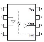
Package Power Dissipation, PD (each channel) ........................200 mWDescriptionThese HCPL-177K units are single, dual, and quad channel, hermetically sealed optocouplers. The HCPL-177K products are capable of operation and storage over the full military temperature range and can be purchased as either standard product or with full MIL-PRF-38534 Class Level H or K testing or from the appropriate DSCC Drawing. All devices are manufactured and tested on a MIL-PRF-38534 certified line and are included in the DSCC Qualified Manufacturers List QML- 38534 for Hybrid Microcircuits.
Each HCPL-177K channel contains a GaAsP light emitting diode which is optically coupled to an integrated high gain photon detector. The high gain output stage features an open collector output providing both lower saturation voltage and
higher signaling speed than possible with conventional photo-Darlington optocouplers. The shallow depth and small junctions offered by the IC process provides better radiation immunity than conventional photo transistor optocouplers.
The supply voltage of HCPL-177K can be operated as low as 2.0 V without adversely affecting the parametric performance.

 HCPL-177K Data Sheet


