GA1085

Features: • Wide frequency range: 24 MHz to 105 MHz• Output configurations: Four outputs at fREF Four outputs at fREF /2 Two outputs at fREF /2 .....with adjustable phase........or Five outputs at 2x fREF Three outputs at fREF Two outputs at fREF ....... with adjustable phase• S...

product image

GA1085 Picture
SeekIC No. : 004347065 Detail

GA1085: Features: • Wide frequency range: 24 MHz to 105 MHz• Output configurations: Four outputs at fREF Four outputs at fREF /2 Two outputs at fREF /2 .....with adjustable phase........or Five ...

floor Price/Ceiling Price

Part Number:
GA1085
Supply Ability:
5000

Price Break

  • Qty
  • 1~5000
  • Unit Price
  • Negotiable
  • Processing time
  • 15 Days
Total Cost: $ 0.00

SeekIC Buyer Protection PLUS - newly updated for 2013!

  • Escrow Protection.
  • Guaranteed refunds.
  • Secure payments.
  • Learn more >>

Month Sales

268 Transactions

Rating

evaluate  (4.8 stars)

Upload time: 2024/10/17

Payment Methods

All payment methods are secure and covered by SeekIC Buyer Protection PLUS.

Notice: When you place an order, your payment is made to SeekIC and not to your seller. SeekIC only pays the seller after confirming you have received your order. We will also never share your payment details with your seller.
Product Details

Description


Features:

• Wide frequency range: 24 MHz to 105 MHz
• Output configurations:
   Four outputs at fREF
   Four outputs at fREF /2
   Two outputs at fREF /2
   .....with adjustable phase........or Five outputs at 2x fREF Three outputs at
   fREF Two outputs at fREF ....... with adjustable phase
• Selectable Phase Shift: 2t, t, +t, and +2t (t = 1/fVCO)
• Low output-to-output skew: 150 ps (max) within a group
• Near-zero propagation delay:
   350 ps +1000 ps (max)
• TTL-compatible with 30 mA output  drive
• 28-pin J-lead surface-mount package


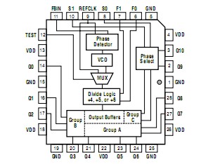
Pinout

  Connection Diagram


Specifications

Storage temperature
65 to +150
Ambient temperature with power applied 2
55 to +100
Supply voltage to ground potential
0.5 V to +7.0 V
DC input voltage
0.5 V to +(VDD + 0.5)
DC input current
30 mA to +5 mA
Package thermal resistance (MQuad)
JA = 45/W
Die junction temperature
TJ = 150


Description

TriQuint's GA1085 is a configurable clock buffer which generates 11 outputs and operates over a wide range of frequencies-from 24 MHz to 105 MHz. The outputs of GA1085 are available at either 1x and 2x or at 1x and  1/2 x the reference clock frequency, fREF. When one of the Group A outputs (Q4Q8) is used as feedback to the PLL, all Group A outputs will be at fREF  , and all Group B (Q0Q3) and Group C (Q9, Q10) outputs will be at  1/2 x fREF  . When one of the Group B outputs is used as feedback to the PLL, all Group A outputs will be at 2x REF and all Group B and Group C outputs will be at fREF  . The Shift Select pins select the phase shift (2t, t, +t or +2t) for Group C outputs (Q9, Q10) with respect to REFCLK. The phase shift increment (t) is equivalent to the VCO's period (1/fVCO).

A very stable internal Phase-Locked Loop (PLL) of GA1085 provides low-jitter operation. This completely self-contained PLL requires no external capacitors or resistors. The PLL's Voltage-Controlled Oscillator (VCO) has a frequency range from 280 MHz to 420 MHz. By feeding back one of the output clocks to FBIN, the PLL continuously maintains frequency and phase synchron-ization between the reference clock (REFCLK) and each of the outputs.

TriQuint's patented output buffer design delivers a very low output-to-output skew of 150 ps (max). The GA1085's symmetrical TTL outputs are capable of sourcing and sinking 30 mA.


Customers Who Bought This Item Also Bought

Margin,quality,low-cost products with low minimum orders. Secure your online payments with SeekIC Buyer Protection.
Isolators
Test Equipment
Undefined Category
Power Supplies - Board Mount
View more