F49L040A

Features: ·Single supply voltage 3.0V-3.6V·Fast access time: 70/90 ns·Compatible with JEDEC standard- Pin-out, packages and software commands compatible with single-power supply Flash·Low power consumption- 7mA typical active current- 25uA typical standby current ·10,000 minimum program/er...

product image

F49L040A Picture
SeekIC No. : 004340058 Detail

F49L040A: Features: ·Single supply voltage 3.0V-3.6V·Fast access time: 70/90 ns·Compatible with JEDEC standard- Pin-out, packages and software commands compatible with single-power supply Flash·Low power cons...

floor Price/Ceiling Price

Part Number:
F49L040A
Supply Ability:
5000

Price Break

  • Qty
  • 1~5000
  • Unit Price
  • Negotiable
  • Processing time
  • 15 Days
Total Cost: $ 0.00

SeekIC Buyer Protection PLUS - newly updated for 2013!

  • Escrow Protection.
  • Guaranteed refunds.
  • Secure payments.
  • Learn more >>

Month Sales

268 Transactions

Rating

evaluate  (4.8 stars)

Upload time: 2024/11/18

Payment Methods

All payment methods are secure and covered by SeekIC Buyer Protection PLUS.

Notice: When you place an order, your payment is made to SeekIC and not to your seller. SeekIC only pays the seller after confirming you have received your order. We will also never share your payment details with your seller.
Product Details

Description


Features:

·Single supply voltage 3.0V-3.6V
·Fast access time: 70/90 ns
·Compatible with JEDEC standard
- Pin-out, packages and software commands compatible with single-power supply Flash
·Low power consumption
- 7mA typical active current
- 25uA typical standby current 
·10,000 minimum program/erase cycles 
·Command register architecture
- Byte programming (9us typical)
- Sector Erase(sector structure: eight 64 KB) 
·Auto Erase (chip & sector) and Auto Program
- Any combination of sectors can be erased concurrently; Chip erase also provided.
- Automatically program and verify data at specified address
·Erase Suspend/Erase Resume
- Suspend or Resume erasing sectors to allow the read/program in another sector
·End of program or erase detection
- Data polling
- Toggle bits
·Sector Protection /Un-protection
- Hardware Protect/Unprotect any combination of sectors from a program or erase operation.
·Low VCC Write inhibit is equal to or less than 2.0V
·Boot Sector Architecture
- U = Upper Boot Sector
- B = Bottom Boot Sector
·Packages available:
- 32-pin TSOPI
- 32-pin PLCC


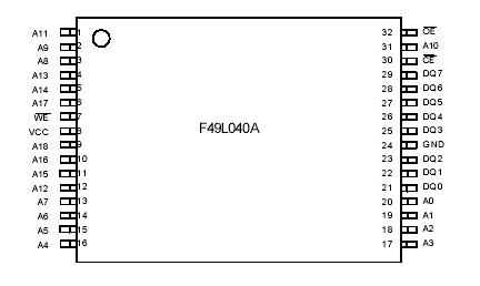
Pinout

  Connection Diagram


Specifications

Plastic Packages . . . . . . . . . . . . . . 65°C to +150°C
Ambient Temperature
with Power Applied. . . . . . . .. . . . . 65°C to +125°C
Voltage with Respect to Ground
VCC (Note 1) . . . . . . . . .. . . .. . . . .. . .0.5 V to +4.0 V
A9 and OE (Note 2) .. . . ... . .. . . . . . 0.5 V to +12.5 V
All other pins (Note 1). . . . . . . . . 0.5 V to VCC +0.5 V
Output Short Circuit Current (Note 3) .. . . . .. . .. 200 mA
Notes:
1. Minimum DC voltage on input or I/O pins is 0.5 V. During voltage transitions, input or I/O pins may overshoot VSS to 2.0 V for periods of up to 20 ns. See Figure

2. Minimum DC input voltage on pins A9 and OE is -0.5 V. During voltage transitions, A9 and OE may overshoot VSS to 2.0 V for periods of up to 20 ns. See Figure 1. Maximum DC input voltage on pin A9 is +12.5 V which may rshoot to 14.0 V for periods up to 20 ns.

3. No more than one output may be shorted to ground at a time. Duration of the short circuit should not be greater than one second.


Description

The F49L040A is a 4 Megabit, 3V only CMOS Flash memory device organized as 512K bytes of 8 bits. This device is packaged in standard 32-pin TSOPI and 32-pin PLCC. It is designed to be programmed and erased both in system and can in standard EPROM programmers.

With access times of 70 ns and 90 ns, the F49L040A allows the operation of high-speed microprocessors. The device has separate chip enable CE , write enable WE  , and output enable OE controls. EFST's memory devices reliably store memory data even after 100,000 program and erase cycles.

The F49L040A is entirely pin and command set compatible with the JEDEC standard for 4 Megabit Flash memory devices. Commands are written to the command register using standard microprocessor write timings.

The F49L040A features a sector erase architecture. The device memory array is divided into eight 64 Kbytes. Sectors can be erased individually or in groups without affecting the data in other sectors. Multiple-sector erase and whole chip erase capabilities provide the flexibility to revise the data in the device.

The sector protect/unprotect feature disables both program and erase operations in any combination of the sectors of the memory. This can be achieved in-system or via programming equipment.

A low VCC detector inhibits write operations on loss of power. End of program or erase is detected by the Data  olling of DQ7, or by the Toggle Bit I feature on DQ6. Once the program or erase cycle has been successfully completed, the device internally resets to the Read mode.


Customers Who Bought This Item Also Bought

Margin,quality,low-cost products with low minimum orders. Secure your online payments with SeekIC Buyer Protection.
Cables, Wires
Optical Inspection Equipment
Hardware, Fasteners, Accessories
Potentiometers, Variable Resistors
Transformers
View more