Features: `COMPLETE CODEC AND FILTERING SYSTEM (DEVICE) INCLUDING: Transmit high-pass and low-pass filtering. Receive low-pass filter with sin x/x correction. Active RC noise filters m-law or A-law compatibleCOder andDECoder. Internal precision voltage reference. Serial I/O interface. Inter...
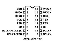
ETC5057-X: Features: `COMPLETE CODEC AND FILTERING SYSTEM (DEVICE) INCLUDING: Transmit high-pass and low-pass filtering. Receive low-pass filter with sin x/x correction. Active RC noise filters m-law or A-...
SeekIC Buyer Protection PLUS - newly updated for 2013!
268 Transactions
All payment methods are secure and covered by SeekIC Buyer Protection PLUS.
Symbol | Parameter |
Value |
Unit |
VCC | VCC to GNDA |
7 |
V |
VBB | VBB to GNDA |
-7 |
V |
VIN, VOUT | Voltage at any Analog Input or Output |
VCC + 0.3 to VBB 0.3 |
V |
Voltage at Any Digital Input or Output |
VCC + 0.3 to GNDA 0.3 |
V | |
Toper | Operating Temperature Range: for ETC5054/57 for ETC5054-X/57-X |
25 to + 125 40 to + 125 |
|
Tstg | Storage Temperature Range |
65 to + 150 |
|
Lead Temperature (soldering, 10 seconds) |
300 |
The ETC5057/ETC5054 family consists of A-law and law monolithic PCM CODEC/filters utilizing the A/D and D/A conversion architecture shown in the block diagram below, and a serial PCM interface.The ETC5057/ETC5054 devices are fabricated using doublepoly CMOS process. The encode portion of each device consists of an input gain adjust amplifier,an active RC pre-filter which eliminates very high frequency noise prior to entering a switched-capacitor band-pass filter that rejects signals below 200 Hz and above 3400 Hz. Also included are auto-zero circuitry and a companding coder which samples the filtered signal and encodes it in the companded A-law or law PCM format. The decode portion of each device ETC5057/ETC5054 consists of an expanding decoder, which reconstructs the analog signal from the companded A-law or law code, a low-pass filter which corrects for the sin x/x response of the decoder output and rejects signals above 3400 Hz and is followed by a single-ended power amplifier capable of driving low impedance loads. The devices require 1.536 MHz, 1.544 MHz, or 2.048 MHz transmit and receive master clocks, which may be asynchronous, transmit and receive bit clocks which may vary from 64 kHz to 2.048 MHz, and transmit and receive frame sync pulses. The timing of the frame sync pulses and PCM data is compatible with both industry standard formats.