Features: • Single power supply operation
- Full voltage range: 2.7 to 3.6 volts read and write operations
• High performance
- Access times as fast as 70 ns
• Low power consumption (typical values at 5 MHz)
- 9 mA typical active read current
- 20 mA typical program/erase current
- Less than 1 A current in standby or automatic sleep mode.
• Flexible Sector Architecture:
- Eight 8-Kbyte sectors, One hundred and twenty-seven 32K-Word / 64K-byte sectors.
- 8-Kbyte sectors for Top or Bottom boot.
- Sector/Sector Group protection:
Hardware locking of sectors to prevent program or erase operations within individual sectors Additionally, temporary Sector Group Unprotect allows code changes in previously locked sectors.
• High performance program/erase speed
- Word program time: 8µs typical
- Sector erase time: 500ms typical
- Chip erase time: 64s typical
• JEDEC Standard compatible
• Standard DATA# polling and toggle bits feature
• Unlock Bypass Program command supported
• Erase Suspend / Resume modes: Read and program another Sector during Erase Suspend Mode
• Support JEDEC Common Flash Interface (CFI).
• Low Vcc write inhibit < 2.5V
• Minimum 100K program/erase endurance cycles.
• RESET# hardware reset pin
- Hardware method to reset the device to read mode.
• WP#/ACC input pin
- Write Protect (WP#) function allows protection of outermost two boot sectors, regardless of sector protect status
- Acceleration (ACC) function provides accelerated program times
• Package Options
- 48-pin TSOP (Type 1)
- 48 ball 6mm x 8mm FBGA
• Commercial and Industrial Temperature Range.
Pinout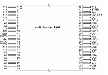 Specifications
| Parameter |
Value |
Unit |
| Storage Temperature |
-65 to +125 |
C |
| Plastic Packages |
-65 to +125 |
C |
Ambient Temperature
With Power Applied |
-55 to +125 |
C |
Output Short Circuit CurrentP 1
|
200 |
MA |
Voltage with
Respect to Ground |
Voltage with
Respect to Ground |
-0.5 to +11.5 |
V |
All other pins 3
|
-0.5 to Vcc+0.5 |
V |
Vcc
|
-0.5 to + 4.0 |
V |
Notes:
1. No more than one output shorted at a time. Duration of the short circuit should not be greater than one second.
2. Minimum DC input voltage on A9, OE#, RESET# and WP#/ACC pins is 0.5V. During voltage transitions, A9, OE#,
RESET# and WP#/ACC pins may undershoot VBssB to 1.0V for periods of up to 50ns and to 2.0V for periods of up to 20ns. See figure below. Maximum DC input voltage on A9, OE#, and RESET# is 11.5V which may overshoot to 12.5V for periods up to 20ns.
3. Minimum DC voltage on input or I/O pins is 0.5 V. During voltage transitions, inputs may undershoot VB
ssB to 1.0V for periods of up to 50ns and to 2.0 V for periods of up to 20ns. See figure below. Maximum DC voltage on output and I/O pins is VB ccB + 0.5 V. During voltage transitions, outputs may overshoot to VB ccB + 1.5 V for periods up to 20ns. See figure below.
4. Stresses above the values so mentioned above may cause permanent damage to the device. These values are for a stress rating only and do not imply that the device should be operated at conditions up to or above these values. Exposure of the device to the maximum rating values for extended periods of time may adversely affect the device reliability.
DescriptionThe EN29LV640T/B is a 64-Megabit, electrically erasable, read/write non-volatile flash memory, organized as 8,388,608 bytes or 4,194,304 words. Any word can be programmed typically in 8µs. The EN29LV640T/B features 3.0V voltage read and write operation, with access times as fast as 70ns to eliminate the need for WAIT states in high-performance microprocessor systems.
The EN29LV640T/B has separate Output Enable (OE#), Chip Enable (CE#), and Write Enable (WE#) controls, which eliminate bus contention issues. This device is designed to allow either single Sector or full Chip erase operation, where each Sector can be individually protected against program/erase operations or temporarily unprotected to erase or program. The device can sustain a minimum of 100K program/erase cycles on each Sector. .

 EN29LV640B Data Sheet