DSP56366

Features: • 120 Million Instructions Per Second (MIPS) with an 120 MHz clock at 3.3V.• Object Code Compatible with the 56K core.• Data ALU with a 24 x 24 bit multiplier-accumulator and a 56-bit barrel shifter. 16-bit arithmetic support.• Program Control with position indepe...

product image

DSP56366 Picture
SeekIC No. : 004329624 Detail

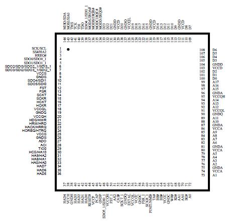
DSP56366: Features: • 120 Million Instructions Per Second (MIPS) with an 120 MHz clock at 3.3V.• Object Code Compatible with the 56K core.• Data ALU with a 24 x 24 bit multiplier-accumulator...

floor Price/Ceiling Price

Part Number:
DSP56366
Supply Ability:
5000

Price Break

  • Qty
  • 1~5000
  • Unit Price
  • Negotiable
  • Processing time
  • 15 Days
Total Cost: $ 0.00

SeekIC Buyer Protection PLUS - newly updated for 2013!

  • Escrow Protection.
  • Guaranteed refunds.
  • Secure payments.
  • Learn more >>

Month Sales

268 Transactions

Rating

evaluate  (4.8 stars)

Upload time: 2024/7/15

Payment Methods

All payment methods are secure and covered by SeekIC Buyer Protection PLUS.

Notice: When you place an order, your payment is made to SeekIC and not to your seller. SeekIC only pays the seller after confirming you have received your order. We will also never share your payment details with your seller.
Product Details

Description


Features:

• 120 Million Instructions Per Second (MIPS) with an 120 MHz clock at 3.3V.
• Object Code Compatible with the 56K core.
• Data ALU with a 24 x 24 bit multiplier-accumulator and a 56-bit barrel shifter. 16-bit arithmetic support.
• Program Control with position independent code support and instruction cache support.
• Six-channel DMA controller.
• PLL based clocking with a wide range of frequency multiplications (1 to 4096), predivider factors (1 to 16) and power saving clock divider (2i: i=0 to 7). Reduces clock noise.
• Internal address tracing support and OnCE for Hardware/Software debugging.
• JTAG port.
• Very low-power CMOS design, fully static design with operating frequencies down to DC.
• STOP and WAIT low-power standby modes.


Pinout

  Connection Diagram


Specifications

Rating1 Symbol Value1, 2 Unit
Supply Voltage VCC −0.3 to +4.0 V
All input voltages excluding "5 V tolerant" inputs3 VIN GND -0.3 to VCC + 0.3 V
All "5 V tolerant" input voltages3 VIN5 GND − 0.3 to VCC + 3.95 V
Current drain per pin excluding VCC and GND I 10 mA
Operating temperature range TJ
Ta
−40 to +105
−40 to +85
°C
Storage temperature TSTG −55 to +125 °C
Notes: 1. GND = 0 V, VCC = 3.3 V ± 0.16 V, TJ = 40°C to +105°C, CL = 50 pF
2. Absolute maximum ratings are stress ratings only, and functional operation at the maximum is not guaranteed.
Stress beyond the maximum rating may affect device reliability or cause permanent damage to the device.
3. CAUTION: All "5 V Tolerant" input voltages must not be more than 3.95 V greater than the supply voltage; this
restriction applies to "power on", as well as during normal operation. In any case, the input voltages cannot be
more than 5.75 V. "5 V Tolerant" inputs are inputs that tolerate 5 V.


Customers Who Bought This Item Also Bought

Margin,quality,low-cost products with low minimum orders. Secure your online payments with SeekIC Buyer Protection.
Optical Inspection Equipment
Discrete Semiconductor Products
Semiconductor Modules
Computers, Office - Components, Accessories
View more