DS90CF366

Features: ·20 to 85 MHz shift clock support·Rx power consumption <142 mW (typ) @85MHz Grayscale·Rx Power-down mode <1.44 mW (max)·ESD rating >7 kV (HBM), >700V (EIAJ)·Supports VGA, SVGA, XGA and Single Pixel SXGA.·PLL requires no external components·Compatible with TIA/EIA-644 LVDS sta...

product image

DS90CF366 Picture
SeekIC No. : 004329335 Detail

DS90CF366: Features: ·20 to 85 MHz shift clock support·Rx power consumption <142 mW (typ) @85MHz Grayscale·Rx Power-down mode <1.44 mW (max)·ESD rating >7 kV (HBM), >700V (EIAJ)·Supports VGA, SVGA,...

floor Price/Ceiling Price

Part Number:
DS90CF366
Supply Ability:
5000

Price Break

  • Qty
  • 1~5000
  • Unit Price
  • Negotiable
  • Processing time
  • 15 Days
Total Cost: $ 0.00

SeekIC Buyer Protection PLUS - newly updated for 2013!

  • Escrow Protection.
  • Guaranteed refunds.
  • Secure payments.
  • Learn more >>

Month Sales

268 Transactions

Rating

evaluate  (4.8 stars)

Upload time: 2024/12/25

Payment Methods

All payment methods are secure and covered by SeekIC Buyer Protection PLUS.

Notice: When you place an order, your payment is made to SeekIC and not to your seller. SeekIC only pays the seller after confirming you have received your order. We will also never share your payment details with your seller.
Product Details

Description


Features:

·20 to 85 MHz shift clock support
·Rx power consumption <142 mW (typ) @85MHz Grayscale
·Rx Power-down mode <1.44 mW (max)
·ESD rating >7 kV (HBM), >700V (EIAJ)
·Supports VGA, SVGA, XGA and Single Pixel SXGA.
·PLL requires no external components
·Compatible with TIA/EIA-644 LVDS standard
·Low profile 56-lead or 48-lead TSSOP package
·DS90CF386 also available in a 64 ball, 0.8mm fine pitch
·ball grid array (FBGA) package


Pinout

  Connection Diagram


Specifications

Supply Voltage (VCC) −0.3V to +4V
CMOS/TTL Output Voltage −0.3V to (VCC + 0.3V)
LVDS Receiver Input Voltage −0.3V to (VCC + 0.3V)
Junction Temperature +150°C
Storage Temperature −65°C to +150°C
Lead Temperature (Soldering, 4 sec for TSSOP)+260°C
Solder Reflow Temperature (Soldering, 20 sec for FBGA) +220°C
Maximum Package Power Dissipation Capacity @25°C
MTD56 (TSSOP) Package: DS90CF386MTD 1.61 W
MTD48 (TSSOP) Package: DS90CF366MTD 1.89 W
Package Derating:
DS90CF386MTD12.4 mW/°C above +25°C
DS90CF366MTD 15 mW/°C above +25°C
Maximum Package Power Dissipation Capacity @ 25°C
SLC64A Package:
DS90CF386SLC 2.0 W
Package Derating:
DS90CF386SLC 10.2 mW/°C above +25°C
ESD Rating
(HBM, 1.5 kΩ, 100 pF) > 7 kV
(EIAJ, 0Ω, 200 pF) > 700V


Description

The DS90CF386 receiver converts the four LVDS data streams (Up to 2.38 Gbps throughput or 297.5 Megabytes/sec bandwidth) back into parallel 28 bits of CMOS/TTL data (24 bits of RGB and 4 bits of Hsync, Vsync, DE and CNTL).

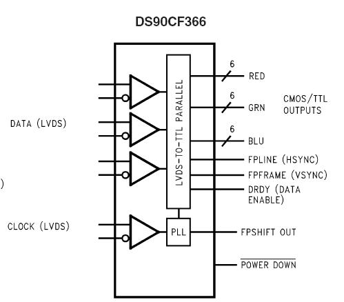
Also available is the DS90CF366 that converts the three LVDS data streams (Up to 1.78 Gbps throughput or 223 Megabytes/sec bandwidth) back into parallel 21 bits of CMOS/TTL data (18 bits of RGB and 3 bits of Hsync, Vsync and DE). Both Receivers' outputs are Falling edge strobe. A Rising edge or Falling edge strobe transmitter (DS90C385/DS90C365) will interoperate with a Falling edge strobe Receiver without any translation logic.

The DS90CF386 is also offered in a 64 ball, 0.8mm fine pitch ball grid array (FBGA) package which provides a 44 % reduction in PCB footprint compared to the 56L TSSOP package.

This chipset DS90CF386 is an ideal means to solve EMI and cable size problems associated with wide, high speed TTL interfaces.


Customers Who Bought This Item Also Bought

Margin,quality,low-cost products with low minimum orders. Secure your online payments with SeekIC Buyer Protection.
Test Equipment
Line Protection, Backups
Semiconductor Modules
Prototyping Products
DE1
Fans, Thermal Management
Connectors, Interconnects
View more