DS90CF364

Features: · 20 to 65 MHz shift clock support· Programmable Transmitter (DS90C363) strobe select (Rising or Falling edge strobe)· Single 3.3V supply· Chipset (Tx + Rx) power consumption < 250 mW (typ)· Power-down mode (< 0.5 mW total)· Single pixel per clock XGA (1024x768) ready· Supports VGA...

product image

DS90CF364 Picture
SeekIC No. : 004329334 Detail

DS90CF364: Features: · 20 to 65 MHz shift clock support· Programmable Transmitter (DS90C363) strobe select (Rising or Falling edge strobe)· Single 3.3V supply· Chipset (Tx + Rx) power consumption < 250 mW (...

floor Price/Ceiling Price

Part Number:
DS90CF364
Supply Ability:
5000

Price Break

  • Qty
  • 1~5000
  • Unit Price
  • Negotiable
  • Processing time
  • 15 Days
Total Cost: $ 0.00

SeekIC Buyer Protection PLUS - newly updated for 2013!

  • Escrow Protection.
  • Guaranteed refunds.
  • Secure payments.
  • Learn more >>

Month Sales

268 Transactions

Rating

evaluate  (4.8 stars)

Upload time: 2024/10/20

Payment Methods

All payment methods are secure and covered by SeekIC Buyer Protection PLUS.

Notice: When you place an order, your payment is made to SeekIC and not to your seller. SeekIC only pays the seller after confirming you have received your order. We will also never share your payment details with your seller.
Product Details

Description


Features:

· 20 to 65 MHz shift clock support
· Programmable Transmitter (DS90C363) strobe select (Rising or Falling edge strobe)
· Single 3.3V supply
· Chipset (Tx + Rx) power consumption < 250 mW (typ)
· Power-down mode (< 0.5 mW total)
· Single pixel per clock XGA (1024x768) ready
· Supports VGA, SVGA, XGA and higher addressability.
· Up to 170 Megabyte/sec bandwidth
· Up to 1.3 Gbps throughput
· Narrow bus reduces cable size and cost
· 290 mV swing LVDS devices for low EMI
· PLL requires no external components
· Low profile 48-lead TSSOP package
· Falling edge data strobe Receiver
· Compatible with TIA/EIA-644 LVDS standard
· ESD rating > 7 kV
· Operating Temperature: −40°C to +85°C


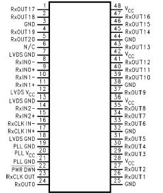
Pinout

  Connection Diagram

  Connection Diagram


Specifications

Function Receiver
Color Depth 18 bpp
Pixel Clock Max 65 MHz
Pixel Clock Min 20 MHz
Input Compatibility LVDS
Output Compatibility LVCMOS
Total Throughput 1365 Mbps
Payload/Channel 455 Mbps
Supply Voltage 3.3 Volt
Temperature Min -40 deg C
Temperature Max 85 deg C
DisplayType FPD
Sensing & Imaging Yes
View Using Catalog


Description

The DS90C363 transmitter converts 21 bits of CMOS/TTL data into three LVDS (Low Voltage Differential Signaling) data streams. A phase-locked transmit clock is transmitted in parallel with the data streams over a fourth LVDS link. Every cycle of the transmit clock 21 bits of input data are sampled and transmitted. The DS90CF364 receiver converts the LVDS data streams back into 21 bits of CMOS/TTL data. At a transmit clock frequency of 65 MHz, 18 bits of RGB data and 3 bits of LCD timing and control data (FPLINE, FPFRAME, DRDY) are transmitted at a rate of 455 Mbps per LVDS data channel. Using a 65 MHz clock, the data throughputs is 170 Mbytes/sec. The Transmitter is offered with programmable edge data strobes for convenient interface with a variety of graphics controllers. The Transmitter can be programmed for Rising edge strobe or Falling edge strobe through a dedicated pin. A Rising edge Transmitter will inter-operate with a Falling edge Receiver (DS90CF364) without any translation logic.

This chipset DS90C363 is an ideal means to solve EMI and cable size problems associated with wide, high speed TTL interfaces.

Reliability Metrics


Part Number Process EFR Reject EFR Sample Size PPM LTA Rejects LTA Device Hours FITS MTTF (Hours)
DS90CF364MTD .35 0 18700 0 0 1290000 3 366041022
DS90CF364MTDX .35 0 18700 0 0 1290000 3 366041022

Note: The Early Failure Rates (EFR) were calculated as point estimate PPM based on rejects and sample size for EFR. The Long Term Failure Rates were calculated at 60% confidence using the Arrhenius equation at 0.7eV activation energy and derating the assumed stress temperature of 150°C to an application temperature of 55°C.

For more information on Reliability Metrics, please click here.


Design Tools


Title Size in Kbytes Date
Evaluation Kit for FPD-Link Family of Serializer and Deserializer LVDS Devices View

If you have trouble printing or viewing PDF file(s), see Printing Problems.

Application Notes


Title Size in Kbytes Date
AN-1085: Application Note 1085 FPD-Link PCB and Interconnect Design-In Guidelines 304 Kbytes 4-Oct-04 Download
AN-1085 (Japanese): Application Note 1085 FPD-Link PCB and Interconnect Design-In Guidelines
640){this.height=this.height*640/this.width;this.width=640;}' border="0" alt=" Connection Diagram">
192 Kbytes

If you have trouble printing or viewing PDF file(s), see Printing Problems.


Customers Who Bought This Item Also Bought

Margin,quality,low-cost products with low minimum orders. Secure your online payments with SeekIC Buyer Protection.
Isolators
Fans, Thermal Management
Transformers
Memory Cards, Modules
Cables, Wires
View more