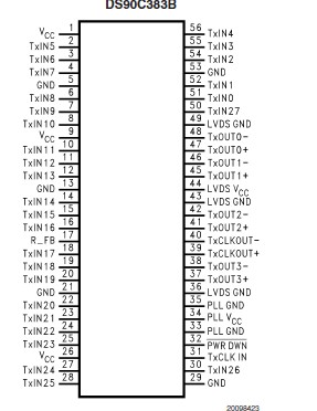
Features: `No special start-up sequence required between clock/data and /PD pins. Input signal (clock and data) can be applied either before or after the device is powered.
`Support Spread Spectrum Clocking up to 100kHz frequency modulation & deviations of ±2.5% center spread or −5% down spread.
`"Input Clock Detection" feature will pull all LVDS pairs to logic low when input clock is missing and when /PD pin is logic high.
`18 to 68 MHz shift clock support
`BestinClass Set & Hold Times on TxINPUTs
`Tx power consumption < 130 mW (typ) @65MHz Grayscale
`40% Less Power Dissipation than BiCMOS Alternatives
`Tx Power-down mode < 60W (typ)
`Supports VGA, SVGA, XGA and Dual Pixel SXGA.
`Narrow bus reduces cable size and cost
`Up to 1.8 Gbps throughput
`Up to 227 Megabytes/sec bandwidth
`345 mV (typ) swing LVDS devices for low EMI
`PLL requires no external components
`Compatible with TIA/EIA-644 LVDS standard
`Low profile 56-lead TSSOP package
`Improved replacement for: SN75LVDS83, DS90C383A
Pinout Specifications
| Function |
Transmitter |
| Color Depth |
24 bpp |
| Pixel Clock Max |
65 MHz |
| Pixel Clock Min |
20 MHz |
| Compression Ratio |
28:4 |
| Input Compatibility |
LVCMOS |
| Output Compatibility |
LVDS |
| Total Throughput |
1820 Mbps |
| Payload/Channel |
455 Mbps |
| Supply Voltage |
3.3 Volt |
| Temperature Min |
-10 deg C |
| Temperature Max |
70 deg C |
| DisplayType |
FPD |
| Sensing & Imaging |
Yes |
| View Using Catalog |
If Military/Aerospace specified devices are required, please contact the National Semiconductor Sales Office/ Distributors for availability and specifications.
Supply Voltage (VCC) ..................−0.3V to +4V
CMOS/TTL Input Voltage ............−0.3V to (VCC + 0.3V)
LVDS Driver Output Voltage ..........−0.3V to (VCC + 0.3V)
LVDS Output Short Circuit
Duration.......................... Continuous
Junction Temperature ....................+150°C
Storage Temperature ...............−65°C to +150°C
Lead Temperature
(Soldering, 4 sec).......................+260°C
Maximum Package Power Dissipation Capacity @ 25°C
MTD56 (TSSOP) Package:
DS90C383B ...........................1.63 W
Package Derating:
DS90C383B ................12.5 mW/°C above +25°C
ESD Rating
(HBM, 1.5 k, 100 pF) .......................7 kV
(EIAJ, 0, 200 pF) .........................500V
DescriptionThe DS90C383B transmitter converts 28 bits of CMOS/TTL data into four LVDS (Low Voltage Differential Signaling) data streams. A phase-locked transmit clock is transmitted in parallel with the data streams over a fifth LVDS link. Every cycle of the transmit clock 28 bits of input data are sampled and transmitted. At a transmit clock frequency of 65 MHz, 24 bits of RGB data and 3 bits of LCD timing and control data (FPLINE, FPFRAME, DRDY) are transmitted at a rate of 455 Mbps per LVDS data channel. Using a 65 MHz clock, the data throughput is 227 Mbytes/sec. The DS90C383B transmitter can be programmed for Rising edge strobe or Falling edge strobe through a dedicated pin. A Rising edge or Falling edge strobe transmitter will interoperate with a Falling edge strobe Receiver (DS90CF386) without any translation logic.
This chipset DS90C383B is an ideal means to solve EMI and cable size problems associated with wide, high speed TTL interfaces.
Reliability Metrics
| Part Number |
Process |
EFR Reject |
EFR Sample Size |
PPM |
LTA Rejects |
LTA Device Hours |
FITS |
MTTF (Hours) |
| DS90C383BMT |
CMOS7 |
0 |
16561 |
0 |
0 |
954000 |
4 |
270700104 |
| DS90C383BMTX |
CMOS7 |
0 |
16561 |
0 |
0 |
954000 |
4 |
270700104 |
| DS90CF383BMT |
CMOS7 |
0 |
16561 |
0 |
0 |
954000 |
4 |
270700104 |
Note: The Early Failure Rates (EFR) were calculated as point estimate PPM based on rejects and sample size for EFR. The Long Term Failure Rates were calculated at 60% confidence using the Arrhenius equation at 0.7eV activation energy and derating the assumed stress temperature of 150°C to an application temperature of 55°C.For more information on Reliability Metrics, please click here.

 DS90C383B Data Sheet


