Features: ` 20 to 65 MHz shift clock support
` Rejects > ± 3ns Jitter from VGA chip with less than 225ps output Jitter @65MHz (TJCC)
` BestinClass Set & Hold Times on TxINPUTs
` Tx power consumption <130 mW (typ) @65MHz Grayscale
` >50% Less Power Dissipation than BiCMOS Alternatives
` Tx Power-down mode <200W (max)
` ESD rating >7 kV (HBM), >500V (EIAJ)
` Supports VGA, SVGA, XGA and Dual Pixel SXGA.
` Narrow bus reduces cable size and cost
` Up to 1.8 Gbps throughput
` Up to 227 Megabytes/sec bandwidth
` 345 mV (typ) swing LVDS devices for low EMI
` PLL requires no external components
` Compatible with TIA/EIA-644 LVDS standard
` Low profile 56-lead TSSOP package
` Improved replacement for:
SN75LVDS83 - DS90C383A
SN75LVDS81 - DS90CF383A
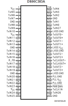
Pinout Specifications
If Military/Aerospace specified devices are required, please contact the National Semiconductor Sales ffice/Distributors for availability and specifications.
Supply Voltage (VCC) .....................................−0.3V to +4V
CMOS/TTL Input Voltage ...................−0.3V to (VCC + 0.3V)
LVDS Driver Output Voltage ..............−0.3V to (VCC + 0.3V)
LVDS Output Short Circuit
Duration Continuous
Junction Temperature ...............................................+150
Storage Temperature ................................−65°C to +150
Lead Temperature
(Soldering, 4 sec) ......................................................+260
Maximum Package Power Dissipation Capacity @ 25
MTD56 (TSSOP) Package:
DS90C383A/DS90CF383A ..........................................1.63 W
Package Derating:
DS90C383A/DS90CF383A .............12.5 mW/ above +25
ESD Rating
(HBM, 1.5 kW, 100 pF) .................................................> 7 kV
(EIAJ, 0W, 200 pF) ......................................................> 500V
DescriptionThe DS90C383A/DS90CF383A transmitter converts 28 bits of CMOS/TTL data into four LVDS (Low Voltage Differential Signaling) data streams. A phase-locked transmit clock is transmitted in parallel with the data streams over a fifth LVDS link. Every cycle of the transmit clock 28 bits of input data are sampled and transmitted. At a transmit clock frequency of 65 MHz, 24 bits of RGB data and 3 bits of LCD timing and control data (FPLINE, FPFRAME, DRDY) are transmitted at a rate of 455 Mbps per LVDS data channel.
Using a 65 MHz clock, the data throughput is 227 Mbytes/sec. The DS90C383A transmitter can be programmed for Rising edge strobe or Falling edge strobe through a dedicated pin. The DS90CF383A is fixed as a Falling edge strobe transmitter. A Rising edge or Falling edge strobe transmitter will interoperate with a Falling edge strobe Receiver (DS90CF384) without any translation logic.
This chipset DS90C383A/DS90CF383A is an ideal means to solve EMI and cable size problems associated with wide, high speed TTL interfaces.

 DS90C383A Data Sheet


