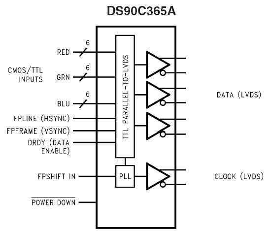
DS90C365A

Features: `Pin-to-pin compatible to DS90C363, DS90C363A and DS90C365 .`No special start-up sequence required between clock/data and /PD pins. Input signals (clock and data) can be applied either before or after the device is powered.`Support Spread Spectrum Clocking up to 100kHz frequency modulati...

product image

DS90C365A Picture
SeekIC No. : 004329321 Detail

DS90C365A: Features: `Pin-to-pin compatible to DS90C363, DS90C363A and DS90C365 .`No special start-up sequence required between clock/data and /PD pins. Input signals (clock and data) can be applied either bef...

floor Price/Ceiling Price

Part Number:
DS90C365A
Supply Ability:
5000

Price Break

  • Qty
  • 1~5000
  • Unit Price
  • Negotiable
  • Processing time
  • 15 Days
Total Cost: $ 0.00

SeekIC Buyer Protection PLUS - newly updated for 2013!

  • Escrow Protection.
  • Guaranteed refunds.
  • Secure payments.
  • Learn more >>

Month Sales

268 Transactions

Rating

evaluate  (4.8 stars)

Upload time: 2024/12/25

Payment Methods

All payment methods are secure and covered by SeekIC Buyer Protection PLUS.

Notice: When you place an order, your payment is made to SeekIC and not to your seller. SeekIC only pays the seller after confirming you have received your order. We will also never share your payment details with your seller.
Product Details

Description


Features:

`Pin-to-pin compatible to DS90C363, DS90C363A and DS90C365 .
`No special start-up sequence required between clock/data and /PD pins. Input signals (clock and data) can be applied either before or after the device is powered.
`Support Spread Spectrum Clocking up to 100kHz frequency modulation & deviations of ±2.5% center spread or -5% down spread.
`"Input Clock Detection" feature will pull all LVDS pairs to logic low when input clock is missing and when /PD pin is logic high.
`18 to 85 MHz shift clock support
`Tx power consumption < 146 mW (typ) @ 85 MHz Grayscale
`Tx Power-down mode < 37 uW (typ)
`Supports VGA, SVGA, XGA, SXGA(dual pixel),
`SXGA+(dual pixel), UXGA(dual pixel).
`Narrow bus reduces cable size and cost
`Up to 1.785 Gbps throughput
`Up to 223.125 Megabytes/sec bandwidth
`345 mV (typ) swing LVDS devices for low EMI
`PLL requires no external components
`Compliant to TIA/EIA-644 LVDS standard
`Low profile 48-lead TSSOP package


Pinout

  Connection Diagram


Specifications

Supply Voltage (VCC)                                                                    −0.3V to +4V
CMOS/TTL Input Voltage                                                  −0.5V to (VCC + 0.3V)
LVDS Driver Output Voltage                                             −0.3V to (VCC + 0.3V)
LVDS Output Short Circuit Duration Continuous
Junction Temperature                                                                          +150°C
Storage Temperature                                                          −65°C to +150°C
Lead Temperature (Soldering, 4 sec)                                                   +260°C
Maximum Package Power Dissipation Capacity @                                    25°C
MTD48 (TSSOP)
Package: DS90C365AMT                                                                        1.98 W
Package Derating: DS90C365AMT                           16 mW/°C above +25°C
ESD Rating
(HBM, 1.5kΩ, 100pF)                                                                                   7kV
(EIAJ, 0Ω, 200 pF)                                                                                     500V
Latch Up Tolerance @                                                               25°C ±100mA


Description

The DS90C365A is a pin to pin compatible replacement for DS90C363, DS90C363A and DS90C365. The DS90C365A has additional features and improvements making it an ideal replacement for DS90C363, DS90C363A and DS90C365. family of LVDS Transmitters.

The DS90C365A transmitter converts 21 bits of LVCMOS/LVTTL data into four LVDS (Low Voltage Differential Signaling) data streams. A phase-locked transmit clock is transmitted in parallel with the data streams over the fourth LVDS link. Every cycle of the transmit clock 21 bits RGB of input data are sampled and transmitted. At a transmit clock frequency of 85 MHz, 21 bits of RGB data and 3 bits of LCD timing and control data (FPLINE, FPFRAME, DRDY) are transmitted at a rate of 595 Mbps per LVDS data channel. Using a 85 MHz clock, the data throughput is 223.125 Mbytes/sec. This transmitter can be programmed for Rising edge strobe or Falling edge strobe through a dedicated pin. A Rising edge or Falling edge strobe transmitter will interoperate with a Falling edge strobe FPDLink Receiver without any translation logic.

This chipset DS90C365A is an ideal means to solve EMI and cable size problems associated with wide, high-speed TTL interfaces with added Spead Spectrum Clocking support..


Customers Who Bought This Item Also Bought

Margin,quality,low-cost products with low minimum orders. Secure your online payments with SeekIC Buyer Protection.
Fans, Thermal Management
Undefined Category
Discrete Semiconductor Products
RF and RFID
View more