Features: ·>155.5 Mbps (77.7 MHz) switching rates
·High impedance LVDS outputs with power-off
·±350 mV differential signaling
·Ultra low power dissipation
·400 ps maximum differential skew (5V, 25°C)
·3.5 ns maximum propagation delay
·Industrial operating temperature range
·Pin compatible with DS26C31, MB571 (PECL) and 41LG (PECL)
·Conforms to ANSI/TIA/EIA-644 LVDS standard
·Offered in narrow and wide body SOIC package
·Fail-safe logic for floating inputsPinout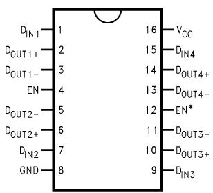 Specifications
| PHY Type |
Line Driver |
| Family |
LVDS |
| Channels |
4 Channels |
| Max Data Rate |
155 Mbps |
| Input Compatibility |
TTL |
| Output Compatibility |
LVDS |
| Power Consumption_ |
20 mW |
| Special Features |
Robust Inputs |
| SupplyVoltage |
5 Volt |
| JTAG1149.1 |
No |
| Temperature Min |
-40 deg C |
| Temperature Max |
85 deg C |
| Function |
Driver |
| View Using Catalog |
Supply Voltage (VCC) −0.3V to +6V
Input Voltage (DIN) −0.3V to (VCC + 0.3V)
Enable Input Voltage (EN, EN*) −0.3V to (VCC + 0.3V)
Output Voltage (DOUT+, DOUT−) −0.3V to +5.8V
Short Circuit Duration (DOUT+, DOUT−) Continuous
Maximum Package Power Dissipation @ +25°C
M Package 1068 mW
WM Package 1562 mW
Derate M Package8.5 mW/°C above +25°C
Derate WM Package 12.5 mW/°C above +25°C
Storage Temperature Range −65°C to +150°C
Lead Temperature Range Soldering (4 sec.) +260°C
Maximum Junction Temperature +150°C
ESD Rating (Note 7)
(HBM, 1.5 kW, 100 pF) 2kV
(EIAJ, 0 W, 200 pF) 250VDescriptionThe DS90C031B is a quad CMOS differential line driver designed for applications requiring ultra low power dissipation and high data rates. The device is designed to support data rates in excess of 155.5 Mbps (77.7 MHz) utilizing Low Voltage Differential Signaling (LVDS) technology.
The DS90C031B accepts TTL/CMOS input levels and translates them to low voltage (350 mV) differential output signals. In addition the driver supports a TRI-STATE function that may be used to disable the output stage, disabling the load current, and thus dropping the device to an ultra low idle power state of 11 mW typical.
In addition, the DS90C031B provides power-off high impedance LVDS outputs. This feature assures minimal loading effect on the LVDS bus lines when VCC is not present.
The DS90C031B and companion line receiver (DS90C032B) provide a new alternative to high power pseudo-ECL devices for high speed point-to-point interface applications.
Reliability Metrics
| Part Number |
Process |
EFR Reject |
EFR Sample Size |
PPM |
LTA Rejects |
LTA Device Hours |
FITS |
MTTF (Hours) |
| DS90C031BTM |
CS080 |
0 |
29095 |
0 |
0 |
2720500 |
2 |
771949303 |
| DS90C031BTMX |
CS080 |
0 |
29095 |
0 |
0 |
2720500 |
2 |
771949303 |
Note: The Early Failure Rates (EFR) were calculated as point estimate PPM based on rejects and sample size for EFR. The Long Term Failure Rates were calculated at 60% confidence using the Arrhenius equation at 0.7eV activation energy and derating the assumed stress temperature of 150°C to an application temperature of 55°C.For more information on Reliability Metrics, please click here.
More Application Notes
| Title |
Size in Kbytes |
Date |
|
| AN-971: Application Note 971 An Overview of LVDS Technology |
168 Kbytes |
5-Oct-98 |
Download |
AN-971 (Japanese): Application Note 971 An Overview of LVDS Technology
640){this.height=this.height*640/this.width;this.width=640;}' border="0" alt=" Connection Diagram"> |
168 Kbytes |
|
|
| AN-1088: Application Note 1088 LVDS Signal Quality: Cable Drive Measurements using Eye Patterns Test Report #3 |
130 Kbytes |
4-Oct-04 |
Download |
| AN-1110: Application Note 1110 LVDS Quad Dynamic I CC vs Frequency |
159 Kbytes |
4-Oct-04 |
Download |
| AN-1040: Application Note 1040 LVDS Performance: Bit Error Rate (BER) Testing Test Report [num]2 |
43 Kbytes |
4-Oct-04 |
Download |
| AN-977: Application Note 977 LVDS Signal Quality: Jitter Measurements Using Eye Patterns Test Report #1 |
63 Kbytes |
5-Oct-98 |
Download |
AN-977 (Japanese): Application Note 977 LVDS Signal Quality: Jitter Measurements Using Eye Patterns Test Report #1
640){this.height=this.height*640/this.width;this.width=640;}' border="0" alt=" Connection Diagram"> |
104 Kbytes |
|
|
If you have trouble printing or viewing PDF file(s), see Printing Problems.
|
The DS90C031B is a quad CMOS differential line driver designed for applications requiring ultra low power dissipation and high data rates. The device is designed to support data rates in excess of 155.5 Mbps (77.7 MHz) utilizing Low Voltage Differential Signaling (LVDS) technology.
The DS90C031B accepts TTL/CMOS input levels and translates them to low voltage (350 mV) differential output signals. In addition the driver supports a TRI-STATE® function that may be used to disable the output stage, disabling the load current, and thus dropping the device to an ultra low idle power state of 11 mW typical.
In addition, the DS90C031B provides power-off high impedance LVDS outputs. This feature assures minimal loading effect on the LVDS bus lines when VCC is not present.
The DS90C031B and companion line receiver (DS90C032B) provide a new alternative to high power pseudo-ECL devices for high speed point-to-point interface applications.

 DS90C031B Data Sheet