Features: ·>155.5 Mbps (77.7 MHz) switching rates
·±350 mV differential signaling
·Ultra low power dissipation
·400 ps maximum differential skew (5V, 25°C)
·3.5 ns maximum propagation delay
·Industrial operating temperature range
·Military operating temperature range option
·Available in surface mount packaging (SOIC) and (LCC)
·Pin compatible with DS26C31, MB571 (PECL) and 41LG (PECL)
·Compatible with IEEE 1596.3 SCI LVDS standard
·Conforms to ANSI/TIA/EIA-644 LVDS standard
·Available to Standard Microcircuit Drawing (SMD) 5962-95833Pinout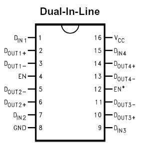 Specifications
Supply Voltage (VCC) −0.3V to +6V
Input Voltage (DIN) −0.3V to (VCC + 0.3V)
Enable Input Voltage (EN, EN*)−0.3V to (VCC + 0.3V)
Output Voltage (DOUT+, DOUT−)−0.3V to (VCC + 0.3V)
Short Circuit Duration (DOUT+, DOUT−) Continuous
Maximum Package Power Dissipation @ +25°C
M Package1068 mW
E Package1900 mW
Derate M Package 8.5 mW/°C above +25°C
Derate E Package12.8 mW/°C above +25°C
Storage Temperature Range −65°C to +150°C
Lead Temperature Range Soldering (4 sec.) +260°C
Maximum Junction Temperature (DS90C031T)+150°C
Maximum Junction Temperature (DS90C031E) +175°C
ESD Rating (Note 7)
(HBM, 1.5 kW, 100 pF) 3,500V
(EIAJ, 0 W, 200 pF) 250V
| PHY Type |
Line Driver |
| Family |
LVDS |
| Channels |
4 Channels |
| Max Data Rate |
155 Mbps |
| Input Compatibility |
TTL |
| Output Compatibility |
LVDS |
| Power Consumption_ |
20 mW |
| SupplyVoltage |
5 Volt |
| JTAG1149.1 |
No |
| Temperature Min |
-40 deg C |
| Temperature Max |
85 deg C |
| Function |
Driver |
| View Using Catalog |
DescriptionThe DS90C031 is a quad CMOS differential line driver designed for applications requiring ultra low power dissipation and high data rates. The device is designed to support data rates in excess of 155.5 Mbps (77.7 MHz) utilizing Low Voltage Differential Signaling (LVDS) technology.
The DS90C031 accepts TTL/CMOS input levels and translates them to low voltage (350 mV) differential output signals. In addition the driver supports a TRI-STATE® function that may be used to disable the output stage, disabling the load current, and thus dropping the device to an ultra low idle power state of 11 mW typical.
The DS90C031 and companion line receiver (DS90C032) provide a new alternative to high power psuedo-ECL devices for high speed point-to-point interface applications.

 DS90C031 Data Sheet