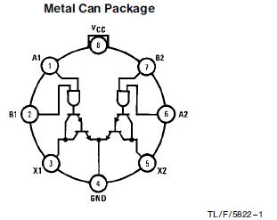
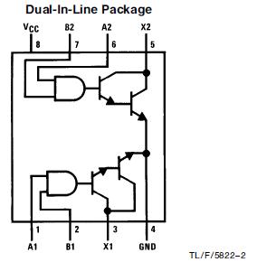
Features: TTL/LS/CMOS compatible inputs
High impedance inputs (PNP's)
High output voltage breakdown (65V typ)
High output current capability (300 mA max)
Internal protection circuit eliminates need for output protection diode
Output breakdown protection if VCC supply is lost
Low VCC power dissipation (90 mW (typ) both outputs "ON'')
Voltage and current levels compatible for use in telephone relay applicationsPinout
 SpecificationsSupply Voltage ............................................................ 7V
Input Voltage .............................................................. 15V
Output Voltage ........................................................... 56V
Storage Temperature Range ...................................... -65 to +150
Maximum Power Dissipation* at 25
Cavity Package ........................................................ 1133 mW
Molded Package ...................................................... 1022 mW
TO-5 Package .......................................................... 787 mW
Lead Temperature (Soldering, 4 seconds) ................ 260
*Derate cavity package 7.6 mW/ above 25; derate molded package 8.2 mW/ above 25; derate TO-5 package 5.2 mW/ above 25.DescriptionThe DS3686 is a high voltage/current positive voltage relay driver having many features not available in present relay drivers.
PNP inputs provide both TTL/LS compatibility and high input impedance for low input loading.
DS3686 Output leakage is specified over temperature at an output voltage of 54V. Minimum output breakdown (ac/latch breakdown) is specified over temperature at 5 mA. This clearly defines the actual breakdown of the device since the circuit has incorporated in it an internal reference which does not allow output breakdown latching found in existing relay drivers. Additionally, this internal reference circuit feature will eliminate the need in most cases of an external clamping (inductive transient voltage protection) diode. When the output is turned "OFF'' by input logic conditions the resulting inductive voltage transient seen at the output is detected by an internal zener reference. The reference then momentarily activates the output transistor long enough so that the relay energy is discharged. This feature eliminates the need of external circuit protection components and insures output transistor protection.
The outputs of DS3686 are Darlington connected transistors, which allow high current operation at low internal V
CC current levelsÐbase drive for the output transistor is obtained from the load in proportion to the required loading conditions. Typical V
CC power with both outputs "ON'' is 90 mW.
The circuit DS3686 also features output transistor protection if the V
CC supply is lost by forcing the output into the high impedance "OFF'' state with the same breakdown levels as when V
CC was applied.

 DS3686 Data Sheet


