Features: · Mil-Std-883C qualified
· Similar to BTL
· Low power ICCL = 41 mA max
· B output controlled ramp rate
· B input noise immunity, typically 4 ns
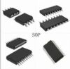
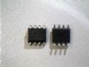
· Available in 28-pin DIP, Flatpak and CLCC
· Pin and function compatible with Signetics 54F776
Pinout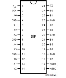 Specifications
The 883 specifications are written to reflect the Rel Electrical Test Specifications (RETS) established by National Semiconductor for this product. For a copy of the latest RETS please contact your local National Semiconductor
sales office or distributor.
Supply Voltage (VCC) .............................................−0.5V to +7.0V
VX, VOH Output Level Control Voltage
(A Outputs) ............................................................−0.5V to +7.0V
OEB n, OEA, LE Input Voltage (VI) .........................−0.5V to +7.0V
A0A7, B0B7 Input Voltage (VI) ...........................−0.5V to +5.5V
Input Current (II) ...............................................−40 mA to +5 mA
Voltage Applied to Output in
High Output State (VO) ........................................−0.5V to +VCCV
A0A7 Current Applied to Output
in Low Output State (IO) .....................................................40 mA
B0B7 Current Applied to Output
in Low Output State (IO) ...................................................200 mA
Storage Temperature Range (TSTG) ....................−65 to +150
Lead Temperature
(Soldering 10 Sec.) ..............................................................260
ESD Tolerance:
CZAP = 120 pF, RZAP = 1500W ...........................................0.5 kV
| Temperature Min |
-55 deg C |
| Temperature Max |
125 deg C |
| Output Mode |
Open Collector |
| Function |
Transceiver |
| View Using Catalog |
DescriptionThe DS1776 is an octal PI-bus Transceiver. The A to B path is latched. B outputs are open collector with series Schottky diode, ensuring minimum B output loading. B outputs also have ramped rise and fall times (2.5 ns typical), ensuring minimum PI-bus ringing. B inputs have glitch rejection circuitry, 4 ns typical.
Designed using National's Bi-CMOS process for both low operating and disabled power. AC performance is optimized for the PI-Bus inter-operability requirements.
The DS1776 is an octal latched transceiver and is intended to provide the electrical interface to a high performance wired-or bus. This bus has a loaded characteristic impedance range of 20W to 50W and is terminated on each end with a 30W to 40W resistor.
The DS1776 is an octal bidirectional transceiver with open collector B and TRI-STATE® A port output drivers. A latch function is provided for the A port signals. The B port output driver is designed to sink 100 mA from 2V and features a controlled linear ramp to minimize crosstalk and ringing on the bus.
A separate high level control voltage (VX) is provided to prevent the A side output high level from exceeding future high density processor supply voltage levels. For 5V systems, VX is tied to VCC.

 DS1776 Data Sheet