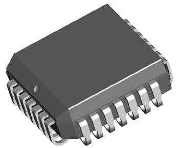
PinoutDescriptionThe DP8571AN is one member of the DP8571A series.The DP8571A is intended for use in microprocessor based systems where information is required for multi-tasking data logging or general time of daydate information.DP8571AN is implemented in low voltage silicon gate microCMOS techno...
DP8571AN: PinoutDescriptionThe DP8571AN is one member of the DP8571A series.The DP8571A is intended for use in microprocessor based systems where information is required for multi-tasking data logging or gene...
SeekIC Buyer Protection PLUS - newly updated for 2013!
268 Transactions
All payment methods are secure and covered by SeekIC Buyer Protection PLUS.
The DP8571AN is one member of the DP8571A series.The DP8571A is intended for use in microprocessor based systems where information is required for multi-tasking data logging or general time of daydate information .DP8571AN is implemented in low voltage silicon gate microCMOS technology to provide low standby power in battery back-up environments.
Features of the DP8571A are:(1)full function real time clock/calendar;(2)programmable multi-function output;(3)internal power supply switch to external battery;(4)automatic log of time into RAM at power failure;(5)INTR/MFO pins programmable HighLow and push-pull or open drain.Time and date are maintained from 1100 of a second to year and leap year in a BCD format 12 or 24 hour modes.Day of week day of month and day of year counters are provided Time is controlled by an on-chip crystal oscillator requiring only the addition of the crystal and two capacitors.The choice of crystal frequency is program selectable.
The absolute maximum ratings of the DP8571A can be summarized as:(1)supply voltage(Vcc):-0.5V to +7.0V;(2)DC input voltage(VIN):-0.5V to Vcc+0.5V;(3)DC output voltage(Vout):-0.5 V to Vcc+0.5V;(4)storage temperature range :-65 to +150°C.The DP8571A's interrupt structure provides four basic types of interrupts Periodic alarm/compare timer and power fail interrupt mask and status registers enable the masking and easy determination of each interrupt.The oscillator is programmed via the Real Time Mode Register to operate at various frequencies.The crystal oscillator is designed to offer optimum performance at each frequency.Thus at 32768 kHz the oscillator is configured as a low frequency and low power oscillator.At the higher frequencies the oscillator inverter oscillator is reconfigured.In addition to the inverter the oscillator feedback bias resistor is included on chip as shown in Figure 4.The oscillator input may be driven from an external source if desired Refer to test mode application note for details The oscillator oscillator stability is enhanced through the use of an on chip regulated power supply.