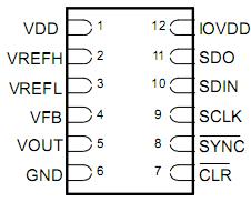
Features: • 2.7-V to 5.5-V Single Supply• 12-Bit Linearity and Monotonicity• Rail-to-Rail Voltage Output• Settling Time: 5 µ s (Max)• Ultralow Glitch Energy: 0.1 nVs• Low Power: 200 µ A (Max)• Power Down: 2 µ A (Max)• Power-On Reset...
DAC7551: Features: • 2.7-V to 5.5-V Single Supply• 12-Bit Linearity and Monotonicity• Rail-to-Rail Voltage Output• Settling Time: 5 µ s (Max)• Ultralow Glitch Energy: 0.1 ...
SeekIC Buyer Protection PLUS - newly updated for 2013!
268 Transactions
All payment methods are secure and covered by SeekIC Buyer Protection PLUS.
UNIT | |
VDD to GND |
-0.3 V to 6 V |
Digital input voltage to GND |
-0.3 V to VDD + 0.3 V |
Vout to GND |
-0.3 V to VDD + 0.3 V |
Operating temperature range |
-40 to 105 |
Storage temperature range |
-65 to 150 |
Junction temperature (TJ Max) |
150 |
The DAC7551 is a single-channel, voltage-output DAC with exceptional linearity and monotonicity. Its proprietary architecture minimizes glitch energy. The low-power DAC7551 operates from a single 2.7-V to 5.5-V supply. The DAC7551 output amplifiers can drive a 2-k Ω , 200-pF load rail-to-rail with 5- µ s settling time; the output range is set using an external voltage reference.
The 3-wire serial interface operates at clock rates up to 50 MHz and is compatible with SPI, QSPI, Microwire ™ , and DSP interface standards. The parts incorporate a power-on-reset circuit to ensure that the DAC outputs power up to zero volts and remain there until a valid write cycle to the device takes place. The parts contain a power-down feature that reduces the current consumption of the device to under 2 µ A.
The small size and low-power operation makes the DAC7551 ideally suited for battery-operated portable applications. The power consumption is typically 0.5 mW at 5 V, 0.23 mW at 3 V, and reduces to 1 µ W.
The DAC7551 is available in a 12-lead SON package and is specified over 40 ° C to 105 ° C.