DAC5686

Features: ` 500 MSPS Maximum Update Rate DAC` WCDMA ACPR 1 Carrier: 76 dB Centered at 30.72-MHz IF,245.76 MSPS 1 Carrier: 73 dB Centered at 61.44-MHz IF,245.76 MSPS 2 Carrier: 72 dB Centered at 30.72-MHz IF,245.76 MSPS 4 Carrier: 64 dB Centered at 92.16-MHz IF,491.52 MSPS` Selectable 2´, ...

product image

DAC5686 Picture
SeekIC No. : 004323690 Detail

DAC5686: Features: ` 500 MSPS Maximum Update Rate DAC` WCDMA ACPR 1 Carrier: 76 dB Centered at 30.72-MHz IF,245.76 MSPS 1 Carrier: 73 dB Centered at 61.44-MHz IF,245.76 MSPS 2 Carrier: 72 dB Centered at 30...

floor Price/Ceiling Price

Part Number:
DAC5686
Supply Ability:
5000

Price Break

  • Qty
  • 1~5000
  • Unit Price
  • Negotiable
  • Processing time
  • 15 Days
Total Cost: $ 0.00

SeekIC Buyer Protection PLUS - newly updated for 2013!

  • Escrow Protection.
  • Guaranteed refunds.
  • Secure payments.
  • Learn more >>

Month Sales

268 Transactions

Rating

evaluate  (4.8 stars)

Upload time: 2024/12/25

Payment Methods

All payment methods are secure and covered by SeekIC Buyer Protection PLUS.

Notice: When you place an order, your payment is made to SeekIC and not to your seller. SeekIC only pays the seller after confirming you have received your order. We will also never share your payment details with your seller.
Product Details

Description


Features:

` 500 MSPS Maximum Update Rate DAC
` WCDMA ACPR
  1 Carrier: 76 dB Centered at 30.72-MHz IF,245.76 MSPS
  1 Carrier: 73 dB Centered at 61.44-MHz IF,245.76 MSPS
   2 Carrier: 72 dB Centered at 30.72-MHz IF,245.76 MSPS
  4 Carrier: 64 dB Centered at 92.16-MHz IF,491.52 MSPS
` Selectable 2´, 4´, 8´, and 16´ Interpolation
  Linear Phase
  0.05-dB Pass-Band Ripple
  80-dB Stop-Band Attenuation
  Stop-Band Transition 0.40.6 fDATA
` 32-Bit Programmable NCO
` On-Chip 2´16´ PLL Clock Multiplier With Bypass Mode
` Differential Scalable Current Outputs: 2 mA to20 mA
` On-Chip 1.2-V Reference
` 1.8-V Digital and 3.3-V Analog Supplies
` 1.8-V/3.3-V CMOS Compatible Interface
` Power Dissipation: 950 mW at Full Maximum Operating Conditions
` Package: 100-Pin HTQFP


Application

` Cellular Base Transceiver Station Transmit Channel
  CDMA: W-CDMA, CDMA2000, IS-95
  TDMA: GSM, IS-136, EDGE/UWC-136
` Baseband I and Q Transmit
` Input Interface: Quadrature Modulation for
  Interfacing With Baseband Complex Mixing ASICs
` Single-Sideband Up-Conversion
` Diversity Transmit
` Cable Modem Termination System


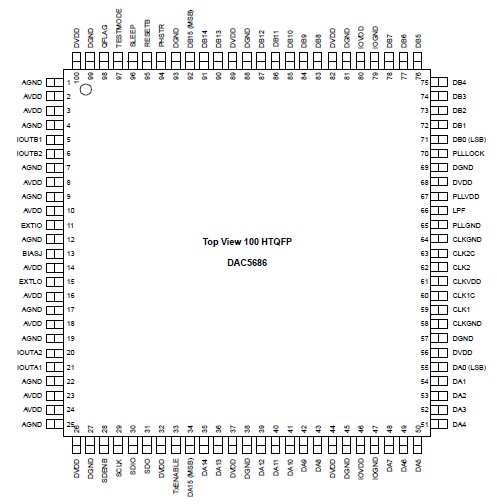
Pinout

  Connection Diagram


Specifications


UNIT

Supply voltage range AVDD(2)

0.5 V to 4 V

DVDD(3)

0.5 V to 2.3 V

CLKVDD(2)

0.5 V to 4 V

IOVDD(2)

0.5 V to 4 V

PLLVDD(2)

0.5 V to 4 V

Voltage between AGND, DGND, CLKGND, PLLGND, and IOGND

0.5 V to 0.5 V

Supply voltage range AVDD to DVDD

0.5 V to 2.6 V

DA[15:0](3)

0.5 V to IOVDD + 0.5 V

DB[15:0](3)

0.5 V to IOVDD + 0.5 V

SLEEP(3)

0.5 V to IOVDD + 0.5 V

CLK1, CLK2, CLK1C, CLK2C(3)

0.5 V to CLKVDD + 0.5 V

RESETB(3)

0.5 V to IOVDD + 0.5 V

LPF(3)

0.5 V to PLLVDD + 0.5 V

IOUT1, IOUT2(2)

1 V to AVDD + 0.5 V

EXTIO, BIASJ(2)

0.5 V to AVDD + 0.5 V

EXTLO(2)

0.5 V to IOVDD + 0.5 V

Peak input current (any input)

±20 mA

Operating free-air temperature range, TA: DAC5686I

40°C to 85°C

Storage temperature range

65°C to 150°C

Lead temperature 1,6 mm (1/16 inch) from the case for 10 seconds

260°C


Description

The DAC5686 is a dual-channel 16-bit high-speed digital-to-analog converter (DAC) with integrated 2´, 4´, 8´, and 16´ interpolation filters, a numerically controlled oscillator (NCO), onboard clock multiplier, and on-chip voltage reference. The DAC5686 has been specifically designed to allow for low input data rates between the DAC and ASIC, or FPGA, and high output transmit intermediate frequencies (IF). Target applications include high-speed digital data transmission in wired and wireless communication systems and high-frequency direct-digital synthesis DDS.

The DAC5686 provides three modes of operation: dual-channel, single-sideband, and quadrature modulation. In dual-channel mode, interpolation filtering increases the DAC update rate, which reduces sinx/x rolloff and enables the use of relaxed analog post-filtering.

Single-sideband mode provides an alternative interface to the analog quadrature modulators. Channel carrier selection is performed at baseband by mixing in the ASIC/FPGA. Baseband I and Q from the ASIC/FPGA are input to the DAC5686, which in turn performs a complex mix resulting in Hilbert transform pairs at the outputs of the DAC5686's two DACs. An external RF quadrature modulator then performs the final single-sideband up-conversion. The DAC5686's complex mixing frequencies are flexibly chosen with the 32-bit programmable NCO.

Unmatched gains and offsets at the RF quadrature modulator result in unwanted sideband and local oscillator feedthrough. Each DAC in the DAC5686 has an 11-bit offset adjustment and 12-bit gain adjustment, which compensate for quadrature modulator input imbalances, thus reducing RF filtering requirements.


Customers Who Bought This Item Also Bought

Margin,quality,low-cost products with low minimum orders. Secure your online payments with SeekIC Buyer Protection.
Prototyping Products
DE1
Crystals and Oscillators
Batteries, Chargers, Holders
Fans, Thermal Management
View more