DAC5652

Features: · 10-Bit Dual Transmit Digital-to-Analog Converter (DAC)· 275 MSPS Update Rate· Single Supply: 3.0 V to 3.6 V· High Spurious-Free Dynamic Range (SFDR): 80 dBc at 5 MHz· High Third-Order Two-Tone Intermodulation (IMD3): 78 dBc at 15.1 MHz and 16.1 MHz· Independent or Single Resistor Gain ...

product image

DAC5652 Picture
SeekIC No. : 004323686 Detail

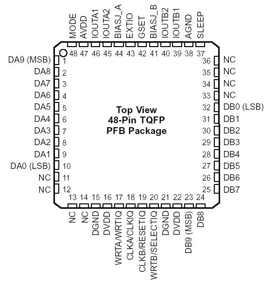
DAC5652: Features: · 10-Bit Dual Transmit Digital-to-Analog Converter (DAC)· 275 MSPS Update Rate· Single Supply: 3.0 V to 3.6 V· High Spurious-Free Dynamic Range (SFDR): 80 dBc at 5 MHz· High Third-Order Tw...

floor Price/Ceiling Price

Part Number:
DAC5652
Supply Ability:
5000

Price Break

  • Qty
  • 1~5000
  • Unit Price
  • Negotiable
  • Processing time
  • 15 Days
Total Cost: $ 0.00

SeekIC Buyer Protection PLUS - newly updated for 2013!

  • Escrow Protection.
  • Guaranteed refunds.
  • Secure payments.
  • Learn more >>

Month Sales

268 Transactions

Rating

evaluate  (4.8 stars)

Upload time: 2024/10/20

Payment Methods

All payment methods are secure and covered by SeekIC Buyer Protection PLUS.

Notice: When you place an order, your payment is made to SeekIC and not to your seller. SeekIC only pays the seller after confirming you have received your order. We will also never share your payment details with your seller.
Product Details

Description


Features:

· 10-Bit Dual Transmit Digital-to-Analog Converter (DAC)
· 275 MSPS Update Rate
· Single Supply: 3.0 V to 3.6 V
· High Spurious-Free Dynamic Range (SFDR): 80 dBc at 5 MHz
· High Third-Order Two-Tone Intermodulation (IMD3): 78 dBc at 15.1 MHz and 16.1 MHz
· Independent or Single Resistor Gain Control
· Dual or Interleaved Data
· On-Chip 1.2-V Reference
· Low Power: 290 mW
· Power-Down Mode: 9 mW
· Package: 48-Pin Thin-Quad Flat Pack (TQFP)


Application

` Cellular Base Transceiver Station Transmit Channel
    CDMA: W-CDMA, CDMA2000, IS-95
    TDMA: GSM, IS-136, EDGE/UWC-136
` Medical/Test Instrumentation
` Arbitrary Waveform Generators (ARB)
` Direct Digital Synthesis (DDS)
` Cable Modem Termination System (CMTS)


Pinout

  Connection Diagram


Specifications

   
UNIT
Supply voltage range AVDD(2)
0.5 V to 4 V
DVDD(3)
0.5 V to 4 V
Voltage between AGND and DGND  
0.5 V to 0.5 V
Voltage between AVDD and DVDD  
0.5 V to 0.5 V
Supply voltage range DA[9:0] and DB[9:0](3)
0.5 V to DVDD + 0.5 V
MODE, CLKA, CLKB, WRTA, WRTB(3)
0.5 V to DVDD + 0.5 V
IOUTA1, IOUTA2, IOUTB1, IOUTB2(2)
1.0 V to AVDD + 0.5 V
EXTIO, BIASJ_A, BIASJ_B, SLEEP(2)
0.5 V to AVDD + 0.5 V
Peak input current (any input)
+20 mA
Peak total input current (all inputs)
30 mA
Operating free-air temperature range
40°C to 85°C
Storage temperature range
65°C to 150°C
Lead temperature 1,6 mm (1/16 inch) from the case for 10 seconds
260°C
(1) Stresses beyond those listed under "absolute maximum ratings" may cause permanent damage to the device. These are stress ratings only and functional operation of these or any other conditions beyond those indicated under "recommended operating conditions" is not implied. Exposure to absolute-maximum-rated conditions for extended periods may affect device reliability.
(2) Measured with respect to AGND.
(3) Measured with respect to DGND.


Description

The DAC5652 is a monolithic, dual-channel, 10-bit, high-speed DAC with on-chip voltage reference.

Operating with update rates of up to 275 MSPS, the DAC5652 offers exceptional dynamic performance, tight-gain, and offset matching characteristics that make it suitable in either I/Q baseband or direct IF communication applications. Each DAC has a high-impedance, differential-current output, suitable for single-ended or differential analog-output configurations. External resistors allow scaling of the full-scale output current for each DAC separately or together, typically between 2 mA and 20 mA. An accurate on-chip voltage reference is temperature-compensated and delivers a stable 1.2-V reference voltage. Optionally, an external reference may be used.

The DAC5652 has two, 10-bit, parallel input ports with separate clocks and data latches. For flexibility, the DAC5652 also supports multiplexed data for each DAC on one port when operating in the interleaved mode. The DAC5652 has been specifically designed for a differential transformer-coupled output with a 50-W doubly-terminated load. For a 20-mA full-scale output current, both a 4:1 impedance ratio (resulting in an output power of 4 dBm) and 1:1 impedance ratio transformer (2 dBm output power) are supported. The DAC5652 is available in a 48-pin TQFP package. Pin compatibility between family members provides 10-bit (DAC5652), 12-bit (DAC5662), and 14-bit (DAC5672) resolution. Furthermore, the DAC5652 is pin compatible to the DAC2900 and AD9763 dual DACs.

The device is characterized for operation over the industrial temperature range of 40°C to 85°C


Customers Who Bought This Item Also Bought

Margin,quality,low-cost products with low minimum orders. Secure your online payments with SeekIC Buyer Protection.
Boxes, Enclosures, Racks
Static Control, ESD, Clean Room Products
Optoelectronics
Prototyping Products
DE1
Industrial Controls, Meters
View more