CY7C603xx

Features: • Powerful Harvard Architecture Processor -M8C Processor Speeds to 12 MHz -Low Power at High Speed -2.4V to 3.6V Operating Voltage -Operating Voltages Down to 1.0V Using On-Chip Switch Mode Pump (SMP) -Commercial Temperature Range: 0°C to +70°C• Configurable Peripherals -8-bi...

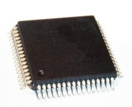
product image

CY7C603xx Picture
SeekIC No. : 004320477 Detail

CY7C603xx: Features: • Powerful Harvard Architecture Processor -M8C Processor Speeds to 12 MHz -Low Power at High Speed -2.4V to 3.6V Operating Voltage -Operating Voltages Down to 1.0V Using On-Chip Swit...

floor Price/Ceiling Price

Part Number:
CY7C603xx
Supply Ability:
5000

Price Break

  • Qty
  • 1~5000
  • Unit Price
  • Negotiable
  • Processing time
  • 15 Days
Total Cost: $ 0.00

SeekIC Buyer Protection PLUS - newly updated for 2013!

  • Escrow Protection.
  • Guaranteed refunds.
  • Secure payments.
  • Learn more >>

Month Sales

268 Transactions

Rating

evaluate  (4.8 stars)

Upload time: 2024/12/21

Payment Methods

All payment methods are secure and covered by SeekIC Buyer Protection PLUS.

Notice: When you place an order, your payment is made to SeekIC and not to your seller. SeekIC only pays the seller after confirming you have received your order. We will also never share your payment details with your seller.
Product Details

Description


Features:

• Powerful Harvard Architecture Processor
   -M8C Processor Speeds to 12 MHz
   -Low Power at High Speed
   -2.4V to 3.6V Operating Voltage
   -Operating Voltages Down to 1.0V Using On-Chip Switch Mode Pump (SMP)
   -Commercial Temperature Range: 0°C to +70°C
• Configurable Peripherals
   -8-bit Timers/Counters/PWM
   -Full Duplex Master or Slave SPI
   -10-bit ADC
   -8-bit Successive Approximation ADC
   -Comparator
• Flexible On-Chip Memory
   -8K Flash Program Storage 50,000 Erase/Write Cycles
   -512 Bytes SRAM Data Storage
   -In-System Serial Programming (ISSP)
   -Partial Flash Updates
   -Flexible Protection Modes
   -EEPROM Emulation in Flash
• Complete Development Tools
   -Free Development Software (PSoC™ Designer)
   -Full-Featured, In-Circuit Emulator and Programmer
   -Complex Breakpoint Structure
   -128K Trace Memory
• Precision, Programmable Clocking
   -Internal ±2.5% 24-/48-MHz Oscillator
   -Internal Oscillator for Watchdog and Sleep
• Programmable Pin Configurations
   -10 mA Drive on All GPIO
   -Pull-up, Pull-down, High Z, Strong, or Open Drain Drive Modes on All GPIO
   -Up to 8 Analog Inputs on GPIO
   -Configurable Interrupt on All GPIO
• Versatile Analog Mux
   -Common Internal Analog Bus
   -Simultaneous Connection of IO Combinations
• Additional System Resources
   -I2C Master, Slave and Multi-Master to 400 kHz
   -Watchdog and Sleep Timers
   -User-Configurable Low Voltage Detection
   -Integrated Supervisory Circuit
   -On-Chip Precision Voltage Reference


Application

• Wireless mice
• Wireless gamepads
• Wireless Presenter tools
• Wireless keypads
• PlayStation® 2 wired gamepads
• PlayStation 2 bridges for wireless gamepads
• Applications requiring a cost effective low voltage 8-bit microcontroller.


Specifications

Parameter
Description
Min.
Typ.
Max.
Unit
Notes
TSTG
Storage Temperature
40
-
+90
°C
Higher storage temperatures will
reduce data retention time.
TA
Ambient Temperature with Power Applied
0
-
+70
°C
 
Vdd
Supply Voltage on Vdd Relative to Vss
0.5
-
5
V
 
VIO
DC Input Voltage
Vss 0.5
-
Vdd + 0.5
V
 
VIOZ
DC Voltage Applied to Tri-state
Vss 0.5
-
Vdd + 0.5
V
 
IMIO
Maximum Current into any Port Pin
25
-
+25
mA
 
ESD
Electro Static Discharge Voltage
2000
-
-
V
Human Body Model ESD.
LU
Latch-up Current
-
-
200
mA


Description

Wireless enCoRe II CY7C603xx device is based on the flexible PSoC architecture. A simple set of peripherals is supported which can be configured as required to match the requirements of each application. Additionally, a fast CPU, Flash program memory, SRAM data memory, and configurable IO are included in a range of convenient pinouts.

This architecture allows the user to create customized peripheral configurations that match the requirements of each individual application. Additionally, a fast CPU, Flash program memory, SRAM data memory, and configurable IO are included in both a 28-pin SSOP and 32-pin QFN packages. Wireless enCoRe II ,CY7C603xx architecture, as illustrated in Figure 1-1, is composed of four main areas: the Wireless enCoRe II(CY7C603xx) Core, the System Resources, Digital System, Analog System and System Resources. Configurable global bus resources allow all the device resources to be combined into a complete custom system. Each Wireless enCoRe II CY7C603xx device supports a limited set of digital and analog peripherals. Depending on the package, up to 28 general purpose IO (GPIO) are also included. The GPIO provide access to the global digital and analog interconnects.


Customers Who Bought This Item Also Bought

Margin,quality,low-cost products with low minimum orders. Secure your online payments with SeekIC Buyer Protection.
Motors, Solenoids, Driver Boards/Modules
Integrated Circuits (ICs)
Inductors, Coils, Chokes
Connectors, Interconnects
View more