Features: • Double high speed, low power, first-in first-out (FIFO) memories
• Double 256 x 9 (CY7C4801)
• Double 512 x 9 (CY7C4811)
• Double 1K x 9 (CY7C4821)
• Double 2K x 9 (CY7C4831)
• Double 4K x 9 (CY7C4841)
• Double 8K x 9 (CY7C4851)
• Functionally equivalent to two CY7C4201/4211/4221/ 4231/4241/4251 FIFOs in a single package
• 0.65 micron CMOS for optimum speed/power
• High-speed 100-MHz operation (10 ns read/write cycle times)
• Offers optimal combination of large capacity, high speed, design flexibility, and small footprint
• Fully asynchronous and simultaneous read and write operation
• Four status flags per device: Empty, Full, and programmable Almost Empty/Almost Full
• Low power - ICC1= 60mA
• Output Enable (OEA/OEB) pins
• Depth Expansion Capabilty
• Width Expansion Capabilty
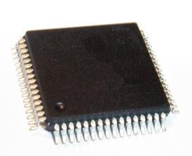
• Space-saving 64-pin TQFP
• Pin compatible and functionally equivalent to IDT72801, 72811, 72821, 72831, 72841,72851Pinout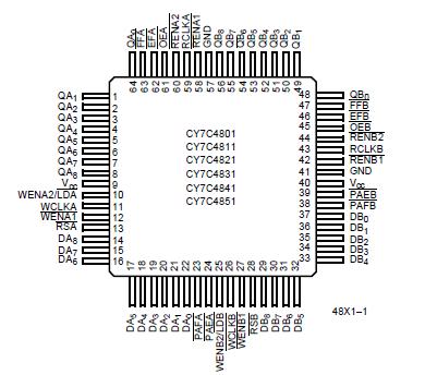 Specifications(Above which the useful life may be impaired. For user guidelines, not tested.)
Storage Temperature ....................................... -65°C to +150°C
Ambient Temperature with
Power Applied.................................................... -55°C to +125°C
Supply Voltage to Ground Potential..................-0.5V to +7.0V
DC Voltage Applied to Outputs
in High Z State.....................................................-0.5V to +7.0V
DC Input Voltage .................................................-0.5V to +7.0V
Output Current into Outputs (LOW) .............................20 mA
Static Discharge Voltage ........................................... >2001V
(per MIL-STD-883, Method 3015)
Latch-Up Current..................................................... >200 mADescriptionThe CY7C48X1 are Double high-speed, low-power, first-in first-out (FIFO) memories with clocked read and write interfaces. The CY7C48X1 are 9 bits wide and operate as two separate FIFOs. The CY7C48X1 are pin-compatible to IDT728X1. Programmable features include Almost Full/Almost Empty flags. These FIFOs provide solutions for a wide variety of data buffering needs, including high-speed data acquisition, multiprocessor interfaces, and communications buffering. These FIFOs have two independent sets of 9-bit input and output ports that are controlled by separate clock and enable signals. The input port is controlled by a free-running clock (WCLKA,WCLKB) and two write-enable pins (WENA1, WENA2/LDA, WENB1, WENB2/LDB).
When (WENA1,WENB1) is LOW and (WENA2/LDA, WENB2/LDB) is HIGH, data is written into the FIFO on the rising edge of the (WCLKA,WCLKB) signal. While (WENA1, WENA2/LDA, WENB1, WENB2/LDB) is held active, data is continually written into the FIFO on each WCLKA, WCLKB cycle. The output port is controlled in a similar manner by a free-running read clock (RCLKA, RCLKB) and two read-enable pins ((RENA1,RENB1), (RENA2,RENB2)). In addition, the CY7C48X1 has output enable pins (OEA, OEB) for each FIFO. The read (RCLKA, RCLKB) and write (WCLKA, WCLKB) clocks may be tied together for single-clock operation or the two clocks may be run independently for asynchronous read/write applications. Clock frequencies up to 100 MHz are achievable.
Depth expansion of the CY7C48X1 is possible using one enable input for system control, while the other enable is controlled by expansion logic to direct the flow of data.
The CY7C48X1 provides two sets of four different status pins: Empty, Full, Almost Empty, Almost Full. The Almost Empty/Almost Full flags are programmable to single word granularity. The programmable flags default to Empty+7 and Full7.
The flags of the CY7C48X1 are synchronous, i.e., they change state relative to either the read clock (RCLKA,RCLKB) or the write clock (WCLKA,WCLKB). When entering or exiting the Empty and Almost Empty states, the flags are updated exclusively by the (RCLKA,RCLKB). The flags denoting Almost Full, and Full states are updated exclusively by (WCLKA,WCLKB) The synchronous flag architecture guarantees that the flags maintain their status for at least one cycle
All configurations of the CY7C48X1 are fabricated using an advanced 0.65m N-Well CMOS technology. Input ESD protection is greater than 2001V, and latch-up is prevented by the use of guard rings.

 CY7C4841 Data Sheet