Features: •8K x 9, 16K x 9, and 32K x 9 FIFO buffer memory
•Asynchronous read/write
•High-speed 33.3-MHz read/write independent of depth/width
•Low operating power
-ICC(max.) = 70 mA
•Programmable Almost Full/Empty flagstatus flags
•Programmable retransmit
•Expandable in width
•5V ±10% supply
•TTL compatible
•Three-state outputs
•Proprietary 0.8-micron CMOS technologyPinout SpecificationsStorage Temperature .................................65°C to +150°C
Ambient Temperature with
Power Applied.............................................55°C to +125°C
Supply Voltage to Ground Potential.....................0.5V to +7.0V
DC Voltage Applied to Outputs
in High Z State.....................................................0.5V to +7.0V
DC Input Voltage.................................................3.0V to +7.0V
Power Dissipation................................................................1.0W
Output Current, into Outputs (LOW)..................................20 mA
Static Discharge Voltage..................................................>2001V
(per MIL-STD-883, Method 3015)
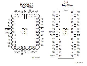
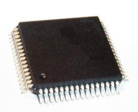
Latch-Up Current............................................................>200 mADescriptionThe CYC47X FIFO series,CY7C470, CY7C472, and CY7C474 consists of high-speed, low-power,first-in first-out (FIFO) memories with programmable flags and retransmit mark. The CY7C470, CY7C472, and CY7C474 are 8K,16K, and 32K words by 9 bits wide, respectively. They areoffered in 600-mil DIP, PLCC, and LCC packages. Each FIFOmemory is organized such that the data is read in the samesequential order that it was written. Three status pins-Emp ty/Full (E/F), Programmable Almost Full/Empty (PAFE), andHalf Full (HF)-are provided to theuser.These pins are de-coded to determine one of six states: Empty, Almost Empty,Less than Half Full, Greater than Half Full, Almost Full, andFull.
The read and write operations of the CY7C470, CY7C472, and CY7C474 may be asynchronous; eachcan occur at a rate of 33.3 MHz. The write operation occurswhen the write (W) signal goes LOW. Read occurs when read(R) goesLOW. The nine data outputs go into a high-imped-ance state when R is HIGH.
The user can store the value of the read pointer for retransmit by using the MARKpin. A LOW on the retransmit (RT) inputcauses the FIFO to resend data by resetting the read pointer to the value stored in the mark pointer.
In the standalone and width expansion configurations, a LOWon the retransmit (RT) input causes the FIFO of the CY7C470, CY7C472, and CY7C474 to resend thedata. With the mark feature, retransmit can start from any word in the FIFO.
The CYC47X series,the CY7C470, CY7C472, and CY7C474 is fabricated using a proprietary 0.8-mi-cron N-well CMOS technology. Input ESD protection is greaterthan 2001V and latch-up is prevented by the use of reliable

 CY7C470 Data Sheet


