Features: • High-speed, low-power, first-in first-out (FIFO) memories
• 8K x 9 FIFO (CY7C460A)
• 16K x 9 FIFO (CY7C462A)
• 32K x 9 FIFO (CY7C464A)
• 64K x 9 FIFO (CY7C466A)
• 10-ns access times, 20-ns read/write cycle times
• High-speed 50-MHz read/write independent of depth/width
• Low operating power
-ICC= 60 mA
-ISB =8 mA
• Asynchronous read/write
• Empty and Full flags
• Half Full flag (in standalone mode)
• Retransmit (in standalone mode)
• TTL-compatible
• Width and Depth Expansion Capability
• 5V ± 10% supply
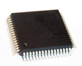
• PLCC, LCC, 300-mil and 600-mil DIP packaging
• Three-state outputs
• Pin compatible density upgrade to CY7C42X/46X family
• Pin compatible and functionally equivalent to IDT7205,
Pinout Specifications(Above which the useful life may be impaired. For user guidelines,
not tested.)
Storage Temperature ..................................65°C to +150°C
Ambient Temperature with
Power Applied..............................................55°C to +125°C
Supply Voltage to Ground Potential .................. 0.5V to +7.0V
DC Voltage Applied to Outputs
in High Z State .................................................. 0.5V to +7.0V
DC Input Voltage............................................... 0.5V to +7.0V
Power Dissipation ..............................................................1.0W
Output Current, into Outputs (LOW)................................ 20 mA
Static Discharge Voltage................................................ >2001V
(per MIL-STD-883, Method 3015)
Latch-Up Current.......................................................... >200 mADescriptionThe CY7C460A, CY7C462A, CY7C464A, and CY7C466A are respectively, 8K, 16K, 32K, and 64K words by 9-bit wide first-in first-out (FIFO) memories. Each FIFO memory is organized such that the data is read in the same sequential order that it was written. Full and Empty flags are provided to prevent overrun and underrun. Three additional pins are also provided to facilitate unlimited expansion in width, depth, or both. The depth expansion technique steers the control signals from one device to another by passing tokens.
The read and write operations of the CY7C460A, CY7C462A, CY7C464A, and CY7C466A may be asynchronous; each can occur at a rate of up to 50 MHz. The write operation occurs when the Write (W) signal is LOW. Read occurs when Read (R) goes LOW. The nine data outputs go to the high-impedance state when R is HIGH.
A Half Full (HF) output flag is provided that is valid in the standalone (single device) and width expansion configurations. In the depth expansion configuration, this pin provides the expansion out (XO) information that is used to tell the next FIFO that it will be activated.
In the standalone and width expansion configurations, a LOW on the Retransmit (RT) input causes the CY7C460A, CY7C462A, CY7C464A, and CY7C466A retransmit the data. Read Enable (R) and Write Enable (W) must both be HIGH during a retransmit cycle, and then R is used to access the data.
The CY7C460A, CY7C462A, CY7C464A, and CY7C466A are fabricated using Cypress's advanced 0.5 RAM3 CMOS technology. Input ESD protection is greater than 2000V and latch-up is prevented by careful layout and the use of guard rings.

 CY7C464A Data Sheet


