Features: • High-speed, low-power, first-in first-out (FIFO) memories
• 512 x 9 (CY7C451)
• 2,048 x 9 (CY7C453)
• 4,096 x 9 (CY7C454)
• 0.65 micron CMOS for optimum speed/power
• High-speed 83-MHz operation (12 ns read/write cycle time)
• Low power - ICC=70 mA
• Fully asynchronous and simultaneous read and write operation
• Empty, Full, Half Full, and programmable Almost Empty and Almost Full status flags
• TTL compatible
• Retransmit function
• Parity generation/checking
• Output Enable (OE) pins
• Independent read and write enable pins
• Center power and ground pins for reduced noise
• Supports free-running 50% duty cycle clock inputs
• Width Expansion Capability
• Depth Expansion Capability
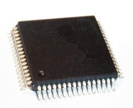
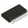
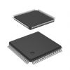
• Available in PLCC packagesPinout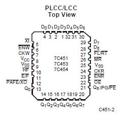 Specifications(Above which the useful life may be impaired. For user guidelines, not tested.)
Storage Temperature ....................................-65°C to +150°C
Ambient Temperature with
Power Applied.................................................-55°C to +125°C
Supply Voltage to Ground Potential .................-0.5V to +7.0V
DC Voltage Applied to Outputs
in High Z State.....................................................-0.5V to +7.0V
DC Input Voltage .................................................-3.0V to +7.0V
Output Current into Outputs (LOW)............................. 20 mA
Static Discharge Voltage ........................................... >2001V
(per MIL-STD-883, Method 3015)
Latch-Up Current.................................................... > 200 mADescriptionThe CY7C451, CY7C453, and CY7C454 are high-speed, low-power, first-in first-out (FIFO) memories with clocked read and write interfaces. The CY7C451, CY7C453, and CY7C454 are 9 bits wide. The CY7C451 has a 512-word by 9-bit memory array, the CY7C453 has a 2048-word by 9-bit memory array, and the CY7C454 has a 4096-word by 9-bit memory array. Devices can be cascaded to increase FIFO depth. Programmable features include Almost Full/Empty flags and generation/checking of parity. These FIFOs provide solutions for a wide variety of data buffering needs, including high-speed data acquisition, multiprocessor interfaces, and communications buffering.
The CY7C451, CY7C453, and CY7C454 have 9-bit input and output ports that are controlled by separate clock and enable signals. The input port is controlled by a free-running clock (CKW) and a write enable pin (ENW). When ENW is asserted, data is written into the FIFO on the rising edge of the CKW signal. While ENW is held active, data is continually written into the FIFO on each CKW cycle. The output port is controlled in a similar manner by a free-running read clock (CKR) and a read enable pin (ENR). The read (CKR) and write (CKW) clocks may be tied together for single-clock operation or the two clocks may be run independently for asynchronous read/write applications. Clock frequencies up to 83.3 MHz are achievable in the standalone configuration, and up to 83.3 MHz is achievable when FIFOs are cascaded for depth expansion.
Depth expansion of the CY7C451, CY7C453, or CY7C454 is possible using the cascade input (XI) and cascade output (XO). The XO signal is connected to the XI of the next device, and the XO of the last device should be connected to the XI of the first device. In standalone mode, the input (XI) pin is simply tied to VSS.
In the standalone and width expansion configurations, a LOW on the retransmit (RT) input causes the CY7C451, CY7C453, and CY7C454 to retransmit the data. Read enable (ENR) and the write enable (ENW) must both be HIGH during the retransmit, and then ENR is used to access the data.

 CY7C453 Data Sheet