CY7C4291V

Features: • 3.3V operation for low power consumption and easy integration into low-voltage systems• High-speed, low-power, first-in first-out (FIFO) memories• 16K * 9 (CY7C4261V)• 32K * 9 (CY7C4271V)• 64K * 9 (CY7C4281V)• 128K * 9 (CY7C4291V)• 0.35-micron ...

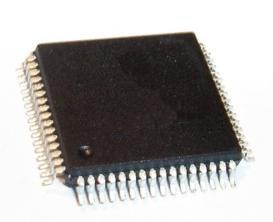
product image

CY7C4291V Picture
SeekIC No. : 004320388 Detail

CY7C4291V: Features: • 3.3V operation for low power consumption and easy integration into low-voltage systems• High-speed, low-power, first-in first-out (FIFO) memories• 16K * 9 (CY7C4261V)&#...

floor Price/Ceiling Price

Part Number:
CY7C4291V
Supply Ability:
5000

Price Break

  • Qty
  • 1~5000
  • Unit Price
  • Negotiable
  • Processing time
  • 15 Days
Total Cost: $ 0.00

SeekIC Buyer Protection PLUS - newly updated for 2013!

  • Escrow Protection.
  • Guaranteed refunds.
  • Secure payments.
  • Learn more >>

Month Sales

268 Transactions

Rating

evaluate  (4.8 stars)

Upload time: 2024/11/21

Payment Methods

All payment methods are secure and covered by SeekIC Buyer Protection PLUS.

Notice: When you place an order, your payment is made to SeekIC and not to your seller. SeekIC only pays the seller after confirming you have received your order. We will also never share your payment details with your seller.
Product Details

Description


Features:

• 3.3V operation for low power consumption and easy integration into low-voltage systems
• High-speed, low-power, first-in first-out (FIFO) memories
• 16K * 9 (CY7C4261V)
• 32K * 9 (CY7C4271V)
• 64K * 9 (CY7C4281V)
• 128K * 9 (CY7C4291V)
• 0.35-micron CMOS for optimum speed/power
• High-speed 100-MHz operation (10-ns read/write cycle times)
• Low power
   -ICC = 25 mA
   -ISB = 4 mA
• Fully asynchronous and simultaneous read and write operation
• Empty, Full, and programmable Almost Empty and Almost Full status flags
• Output Enable (OE) pin
• Independent read and write enable pins
• Supports free-running 50% duty cycle clock inputs
• Width- Expansion capability
• 32-pin PLCC
• Pin-compatible density upgrade to CY7C42X1V family
• Pin-compatible 3.3V solutions for CY7C4261/71/81/91


Pinout

  Connection Diagram


Specifications

(Above which the useful life may be impaired. For user guidelines, not tested.)
Storage Temperature ...................................65 to +150
Ambient Temperature with
Power Applied...............................................55 to +125
Supply Voltage to Ground Potential .............. 0.5V to +3.6V
DC Voltage Applied to Outputs
in High-Z State ........................................0.5V to VCC + 0.5V
DC Input Voltage ................................... 0.5V to VCC + 0.5V
Output Current into Outputs (LOW).............................. 20 mA
Static Discharge Voltage............................................ > 2001V
(per MIL-STD-883, Method 3015)
Latch-up Current...................................................... > 200 mA


Description

The CY7C4261/71/81/91V are high-speed, low-power FIFO memories with clocked read and write interfaces. The  CY7C4261/71/81/91V are nine bits wide. The CY7C4261/71/81/91V are pin-compatible to the CY7C42x1V Synchronous FIFO family. Programmable features include Almost Full/Almost Empty flags. The CY7C4261/71/81/91V provide solutions for a wide variety of data buffering needs, including high-speed data acquisition, multiprocessor interfaces, and communications buffering.

The CY7C4261/71/81/91V  have 9-bit input and output ports that are controlled by separate clock and enable signals. The input port is controlled by a free-running clock (WCLK) and two write-enable pins (WEN1, WEN2/LD).

When WEN1 is LOW and WEN2/LD is HIGH, data is written into the FIFO of the CY7C4261/71/81/91V on the rising edge of the WCLK signal. While WEN1 and WEN2/LD are held active, data is continually written into the FIFO on each WCLK cycle. The output port is controlled in a similar manner by a free-running read clock (RCLK) and two read enable pins (REN1, REN2). In addition,the CY7C4261/71/81/91V has an output enable pin (OE). The read (RCLK) and write (WCLK) clocks may be tied together for single-clock operation or the two clocks may be run independently for asynchronous read/write applications. Clock frequencies up to 100 MHz are achievable. Depth expansion is possible using one enable input for system control, while the other enable is controlled by expansion logic to direct the flow of data.


Customers Who Bought This Item Also Bought

Margin,quality,low-cost products with low minimum orders. Secure your online payments with SeekIC Buyer Protection.
Boxes, Enclosures, Racks
Memory Cards, Modules
Audio Products
Motors, Solenoids, Driver Boards/Modules
View more