CY7C1460AV25

Features: • Pin-compatible and functionally equivalent to ZBT™• Supports 250-MHz bus operations with zero wait states- Available speed grades are 250, 200 and 167 MHz• Internally self-timed output buffer control to eliminate the need to use asynchronous OE• Fully regi...

product image

CY7C1460AV25 Picture
SeekIC No. : 004320159 Detail

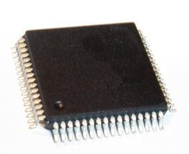
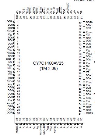
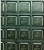
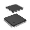
CY7C1460AV25: Features: • Pin-compatible and functionally equivalent to ZBT™• Supports 250-MHz bus operations with zero wait states- Available speed grades are 250, 200 and 167 MHz• Intern...

floor Price/Ceiling Price

Part Number:
CY7C1460AV25
Supply Ability:
5000

Price Break

  • Qty
  • 1~5000
  • Unit Price
  • Negotiable
  • Processing time
  • 15 Days
Total Cost: $ 0.00

SeekIC Buyer Protection PLUS - newly updated for 2013!

  • Escrow Protection.
  • Guaranteed refunds.
  • Secure payments.
  • Learn more >>

Month Sales

268 Transactions

Rating

evaluate  (4.8 stars)

Upload time: 2024/5/22

Payment Methods

All payment methods are secure and covered by SeekIC Buyer Protection PLUS.

Notice: When you place an order, your payment is made to SeekIC and not to your seller. SeekIC only pays the seller after confirming you have received your order. We will also never share your payment details with your seller.
Product Details

Description


Features:

• Pin-compatible and functionally equivalent to ZBT™
• Supports 250-MHz bus operations with zero wait states
- Available speed grades are 250, 200 and 167 MHz
• Internally self-timed output buffer control to eliminate the need to use asynchronous OE
• Fully registered (inputs and outputs) for pipelined operation
• Byte Write capability
• 2.5V core power supply
• 2.5V/1.8V I/O operation
• Fast clock-to-output times
- 2.6 ns (for 250-MHz device)
- 3.2 ns (for 200-MHz device)
- 3.4 ns (for 167-MHz device)
• Clock Enable (CEN) pin to suspend operation
• Synchronous self-timed writes
• CY7C1460AV25, CY7C1462AV25 available in JEDEC-standard lead-free 100-pin TQFP package, lead-free and non-lead-free 165-ball FBGA package. CY7C1464AV25 available in lead-free and non-lead-free 209-ball FBGA package
• IEEE 1149.1 JTAG Boundary Scan
• Burst capability-linear or interleaved burst order
• "ZZ" Sleep Mode option and Stop Clock option


Pinout

  Connection Diagram


Specifications

(Above which the useful life may be impaired. For user guidelines, not tested.)
Storage Temperature .................................65°C to +150°C
Ambient Temperature with
Power Applied.............................................55°C to +125°C
Supply Voltage on VDD Relative to GND........ 0.5V to +3.6V
DC to Outputs in Tri-State ................... 0.5V to VDDQ + 0.5V
DC Input Voltage....................................0.5V to VDD + 0.5V
Current into Outputs (LOW)......................................... 20 mA
Static Discharge Voltage.......................................... > 2001V
(per MIL-STD-883, Method 3015)
Latch-up Current.................................................... > 200 mA


Description

The CY7C1460AV25/CY7C1462AV25/CY7C1464AV25 are 2.5V, 1M x 36/2M x 18/512 x 72 Synchronous pipelined burst SRAMs with No Bus Latency™ (NoBL™) logic, respectively.

They are designed to support unlimited true back-to-back Read/Write operations with no wait states. The CY7C1460AV25/CY7C1462AV25/CY7C1464AV25 are equipped with the advanced (NoBL) logic required to enable consecutive Read/Write operations with data being transferred on every clock cycle. This feature dramatically improves the throughput of data in systems that require frequent Write/Read transitions. The CY7C1460AV25/ CY7C1462AV25/ CY7C1464AV25 are pin-compatible and functionally equivalent to ZBT devices.

All synchronous inputs pass through input registers controlled by the rising edge of the clock. All data outputs pass through output registers controlled by the rising edge of the clock. The clock input is qualified by the Clock Enable (CEN) signal, which when deasserted suspends operation and extends the previous clock cycle. Write operations are controlled by the Byte Write Selects (BWaBWh for CY7C1464AV25, BWaBWd for CY7C1460AV25 and BWaBWb for CY7C1462AV25) and a Write Enable (WE) input. All writes are conducted with on-chip synchronous self-timed write circuitry.

Three synchronous Chip Enables (CE1, CE2, CE3) and an asynchronous Output Enable (OE) of CY7C1460AV25/CY7C1462AV25/CY7C1464AV25 provide for easy bank selection and output three-state control. In order to avoid bus contention, the output drivers are synchronously three-stated during the data portion of a write sequence.


Customers Who Bought This Item Also Bought

Margin,quality,low-cost products with low minimum orders. Secure your online payments with SeekIC Buyer Protection.
Connectors, Interconnects
Sensors, Transducers
Power Supplies - Board Mount
Tapes, Adhesives
803
View more