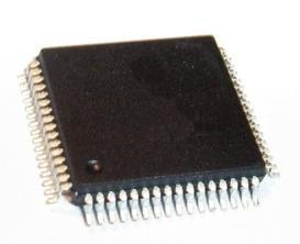
Organization
:
Packaging
:
Mounting Style
: SMD/SMT
Access Time
: 0.45 ns
Supply Voltage - Max
: 1.9 V
Supply Voltage - Min
: 1.7 V
Maximum Operating Temperature
: + 70 C
Minimum Operating Temperature
: 0 C
Memory Size
: 18 Mbit
Package / Case
: FBGA
Maximum Operating Current
: 865 mA
Description
The CY7C1393JV18-300BZXC is a type of 1.8V Synchronous Pipelined SRAMs And CY7C1393JV18-300BZXC is equipped with Double Data Ra te Separate IO (DDR-II SIO)architecture. The DDR-II SIO contains two separate ports: one is the read port, and the other is the write port to access the memory array. The DDR-II SIO has departed data inputs and data outputs to fully eliminate the need to 'turnaround' the data bus demanded with common IO devices. Access to each port is acc omplished via a common address bus. Write data is recorded on the rising edges of both K and K. Read data is drive n on the rising edges of C and C if offered, or on the rising edge of K and K if C or C is not offered. Each address loc ation is combined with 18-bit words that burst sequentially into or out of the device.
Features of the CY7C1393JV18-300BZXC are:(1) 300 MHz clock for high bandwidth;(2) 2-word burst for reducing add ress bus frequency;(3)double data rate (DDR) interfaces(data transferred at 600 MHz) at 300 MHz;(4)two input cloc ks (K and K) for precise DDR timing:SRAM uses rising edges only;(5)two input clocks for output data (C and C) to mi nimize clock skew and flight time mismatches;(6)echo clocks (CQ and CQ) simplify data capture in high speed system s;(7)synchronous internally self-timed writes;(8)operates similar to a DDR-I device with one cycle read latency in DLL off mode;(9)1.8V core power supply with HSTL inputs and outputs.
The absolute maximum ratings of the CY7C1393JV18-300BZXC can be summarized as:(1):storage temperature rang es from65°C to +150°C;(2):ambient temperature with power applied is55°C to +125°C;(3):supply voltage on VDD relative to GND is0.5V to +2.9V;(4):DC voltage applied to outputs in high-Z state is0.5V to VDDQ + 0.3V;(5): DC input voltage is0.5V to VDD + 0.3V;(6):current into outputs (LOW)is 20 mA;(7):static discharge voltage(MIL-STD 883, Method 3015)is greater than 2001V;(8):latch up current is greater than 200 mA;(9)supply voltage on VDDQ rel tive to GND is0.5V to +VDD.
Parameters: | Technical/Catalog Information | CY7C1393JV18-300BZXC |
| Vendor | Cypress Semiconductor Corp |
| Category | Integrated Circuits (ICs) |
| Memory Type | SRAM - Synchronous |
| Memory Size | 18M (1M x 18) |
| Speed | 300MHz |
| Interface | Parallel |
| Package / Case | 165-FBGA |
| Packaging | Tray |
| Voltage - Supply | 1.7 V ~ 1.9 V |
| Operating Temperature | 0°C ~ 70°C |
| Format - Memory | RAM |
| Lead Free Status | Lead Free |
| RoHS Status | RoHS Compliant |
| Other Names | CY7C1393JV18 300BZXC
CY7C1393JV18300BZXC
|

 CY7C1393JV18-300BZXC Data Sheet


