Features: • Zero Bus Latency, no dead cycles between Write and Read cycles
• Fast clock speed: 200, 167, 150, and 133 MHz
• Fast access time: 3.0, 3.4, 3.8, and 4.2 ns
• Internally synchronized registered outputs eliminate the need to control OE
• Single 3.3V 5% and +10% power supply VDD
• Separate VDDQ for 3.3V or 2.5V I/O
• Single WE (Read/Write) control pin
• Positive clock-edge triggered address, data, and control signal registers for fully pipelined applications
• Interleaved or linear four-word burst capability
• Individual byte Write (BWSaBWSd) control (may be tied LOW)
• CEN pin to enable clock and suspend operations
• Three chip enables for simple depth expansion
• JTAG boundary scan (BGA package only)
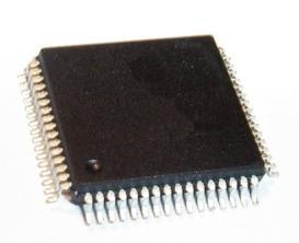
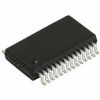
• Available in 119-ball bump BGA and 100-pin TQFP packages
• Automatic power down available using ZZ mode or CE deselect
Pinout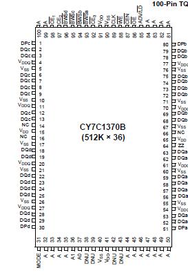 Specifications(Above which the useful life may be impaired. For user guidelines,
not tested.)
Storage Temperature ..................................65 to +150
Ambient Temperature with
Power Applied............................................. 55 to +125
Supply Voltage on VDD Relative to GND ....... 0.5V to +4.6V
DC Voltage Applied to Outputs
in High Z State[13] ............................. 0.5V to VDDQ + 0.5V
DC Input Voltage[13] ..........................0.5V to VDDQ + 0.5V
Current into Outputs (LOW) ...................................... 20 mA
Static Discharge Voltage ......................................... >1500V
(per MIL-STD-883, Method 3015)
Latch-Up Current................................................... >200 mADescriptioneliminate dead cycles CY7C1370B when transitions from Read to Write or vice versa. These SRAMs are optimized for 100 percent bus utilization and achieve Zero Bus Latency. They integrate 524,288 × 36 and 1,048,576 × 18 SRAM cells, respectively, with advanced synchronous peripheral circuitry and a 2-bit counter for internal burst operation. The Synchronous Burst SRAM CY7C1370B family employs high-speed, low-power CMOS designs using advanced single-layer polysilicon, three-layer metal technology. Each memory cell consists of six transistors.
All synchronous inputs of CY7C1370B are gated by registers controlled by a positive-edge-triggered Clock input (CLK). The synchronous inputs include all addresses, all data inputs, depth-expansion Chip Enables (CE1, CE2, and CE3), cycle start input CY7C1370B (ADV/LD), Clock enable (CEN), byte Write Enables (BWSa, BWSb, BWSc, and BWSd), and Read-Write Control (WE). BWSc and BWSd apply to CY7C1370B only.
Address and control signals of CY7C1370B are applied to the SRAM during one clock cycle, and two cycles later, its associated data occurs, either Read or Write.
A Clock enable (CEN) pin of CY7C1370B allows operation of the CY7C1370B/CY7C1372B to be suspended as long as necessary. All synchronous inputs are ignored when CEN is HIGH and the internal device registers will hold their previous values.
There are three chip enable pins (CE1, CE2, CE3) CY7C1370B allow the user to deselect the device when desired. If any one of these three are not active when ADV/LD is LOW, no new memory operation of CY7C1370B can be initiated and any burst cycle in progress is stopped. However, any pending data transfers (Read or Write) will be completed. The data bus will be in high-impedance state two cycles after the chip is deselected or a Write cycle is initiated.
The CY7C1370B and CY7C1372B have an on-chip two-bit burst counter. In the burst mode, the CY7C1370B and CY7C1372B provide four cycles of data for a single address presented to the SRAM. The order of the burst sequence is defined by the MODE input pin. The MODE pin selects between linear and interleaved burst sequence. The ADV/LD signal is used to load a new external address (ADV/LD = LOW) or increment the internal burst counter (ADV/LD = HIGH) Output enable (OE) and burst sequence select (MODE) are the asynchronous signals. OE can be used to disable the outputs at any given time. ZZ may be tied to LOW if it is not used.
Four pins of CY7C1370B are used to implement JTAG test capabilities. The JTAG circuitry is used to serially shift data to and from the device. JTAG inputs use LVTTL/LVCMOS levels to shift data during this testing mode of operation.

 CY7C1370B Data Sheet