Packaging
: Tray
Mounting Style
: SMD/SMT
Supply Voltage - Max
: 3.6 V
Maximum Operating Temperature
: + 85 C
Minimum Operating Temperature
: - 40 C
Supply Voltage - Min
: 3.135 V
Package / Case
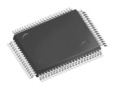
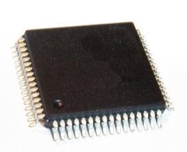
: TQFP-100
Memory Size
: 9 Mbit
Organization
: 256 K x 36
Maximum Operating Current
: 40 mA
Access Time
: 3.5 ns
DescriptionThe CY7C1354C-166AXI is one member of the CY7C1354C family which is designed as the 3.3V, 256K x 36 and 512K x 18 synchronous pipelined burst SRAM CY7C1354C-166AXI that is equipped with the advanced (NoBL) logic required to enable consecutive Read/Write operations with data being transferred on every clock cycle. And in order to avoid bus contention, the output drivers are synchronously tri-stated during the data portion of a write sequence.
Features of the CY7C1354C-166AXI are:(1)internally self-timed output buffer control to eliminate the need to use asynchronous OE; (2)fully registered (inputs and outputs) for pipelined operation; (3)byte Write capability; (4)single 3.3V power supply (VDD); (5)3.3V or 2.5V I/O power supply (VDDQ); (6)fast clock-to-output times; (7)2.8 ns (for 250-MHz device); (8)Clock Enable (CEN) pin to suspend operation; (9)synchronous self-timed writes; (10)available in lead-free 100-Pin TQFP package, lead-free and non lead-free 119-ball BGA package and 165-ball FBGA package; (11)IEEE 1149.1 JTAG-compatible boundary scan; (12)burst capability-linear or interleaved burst order; (13)"ZZ" sleep mode option and stop clock option; (14)pin-compatible and functionally equivalent to ZBT.
The absolute maximum ratings of the CY7C1354C-166AXI can be summarized as:(1)storage temperature:-65°C to +150°C;(2)ambient temperature with power applied:-55°C to +125°C;(3)supply voltage on VDD relative to GND:-0.5V to +4.6V;(4)supply voltage on VDDQ relative to GND:-0.5V to +VDD;(5)DC to outputs in Tri-State:-0.5V to VDDQ+0.5V;(6)DC input voltage:0.5V to VDD + 0.5V;(7)current into outputs (LOW):20 mA;(8)latch-up current:>200 mA. If you want to know more information such as the electrical characteristics about the CY7C1354C-166AXI, please download the datasheet in www.seekic.com or www.chinaicmart.com .
Parameters: | Technical/Catalog Information | CY7C1354C-166AXI |
| Vendor | Cypress Semiconductor Corp |
| Category | Integrated Circuits (ICs) |
| Memory Type | SRAM - Synchronous |
| Memory Size | 9M (256K x 36) |
| Speed | 166MHz |
| Interface | Parallel |
| Package / Case | 100-TQFP |
| Packaging | Tray |
| Voltage - Supply | 3.135 V ~ 3.6 V |
| Operating Temperature | -40°C ~ 85°C |
| Format - Memory | RAM |
| Lead Free Status | Lead Free |
| RoHS Status | RoHS Compliant |
| Other Names | CY7C1354C 166AXI
CY7C1354C166AXI
428 2119 ND
4282119ND
428-2119
|

 CY7C1354C-166AXI Data Sheet


