Features: Can support up to 133-MHz bus operations with zero wait states Data is transferred on every clock
Pin compatible and functionally equivalent to ZBT™ devices
Internally self-timed output buffer control to eliminate the need to use OE
Registered inputs for flow-through operation
Byte Write capability
128K x 36 common I/O architecture
2.5V / 3.3V I/O power supply
Fast clock-to-output times 6.5 ns (for 133-MHz device) 7.5 ns (for 117-MHz device) 8.0 ns (for 100-MHz device) 11.0 ns (for 66-MHz device)
Clock Enable (CEN) pin to suspend operation
Synchronous self-timed writes
Asynchronous Output Enable
JEDEC-standard 100 TQFP and 119 BGA packages
Burst Capability-linear or interleaved burst order
Low standby power
Pinout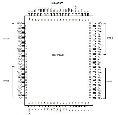 Specifications
(Above which the useful life may be impaired. For user guidelines, not tested.)
Storage Temperature ..........................................65 to +150
Ambient Temperature with
Power Applied......................................................55 to +125
Supply Voltage on VDD Relative to GND ............... 0.5V to +4.6V
DC Voltage Applied to Outputs
in three-state ............................................ 0.5V to VDDQ + 0.5V
DC Input Voltage...........................................0.5V to VDD + 0.5V
Current into Outputs (LOW)................................................ 20 mA
Static Discharge Voltage.................................................. > 2001V
(per MIL-STD-883, Method 3015)
Latch-up Current............................................................ > 200 mA
DescriptionThe CY7C1351F is a 3.3V, 128K x 36 Synchronous Flow-through Burst SRAM designed specifically to support unlimited true back-to-back Read/Write operations without the insertion of wait states. The CY7C1351F is equipped with the advanced No Bus Latency™ (NoBL™) logic required to enable consecutive Read/Write operations with data being transferred on every clock cycle. This feature dramatically improves the throughput of data through the SRAM, especially in systems that require frequent Write-Read transitions.
All synchronous inputs of CY7C1351F pass through input registers controlled by the rising edge of the clock. The clock input is qualified by the Clock Enable (CEN ) signal, which when deasserted suspends operation and extends the previous clock cycle. Maximum access delay from the clock rise is 6.5 ns (133-MHz device).
Write operations of CY7C1351F are controlled by the four Byte Write Select (BW[A:D]) and a Write Enable (WE) input. All writes are conducted with on-chip synchronous self-timed write circuitry.
Three synchronous Chip Enables (CE1, CE2, CE3) and an asynchronous Output Enable (OE )of CY7C1351F provide for easy bank selection and output three-state control. In order to avoid bus contention, the output drivers CY7C1351F are synchronously three-stated during the data portion of a write sequence.

 CY7C1351F Data Sheet