Features: Registered inputs and outputs for pipelined operation
256K *18 common I/O architecture
3.3V core power supply
3.3V / 2.5V I/O operation
Fast clock-to-output times
- 2.6 ns (for 250-MHz device)
- 2.6 ns (for 225-MHz device)
- 2.8 ns (for 200-MHz device)
- 3.5 ns (for 166-MHz device)
- 4.0 ns (for 133-MHz device)
- 4.5 ns (for 100-MHz device)
Provide high-performance 3-1-1-1 access rate
User-selectable burst counter supporting Intel
Pentium interleaved or linear burst sequences
Separate processor and controller address strobes
Synchronous self-timed writes
Asynchronous output enable
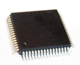
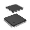
Offered in JEDEC-standard 100-pin TQFP and 119 Ball
BGA packages.
"ZZ" Sleep Mode OptionPinout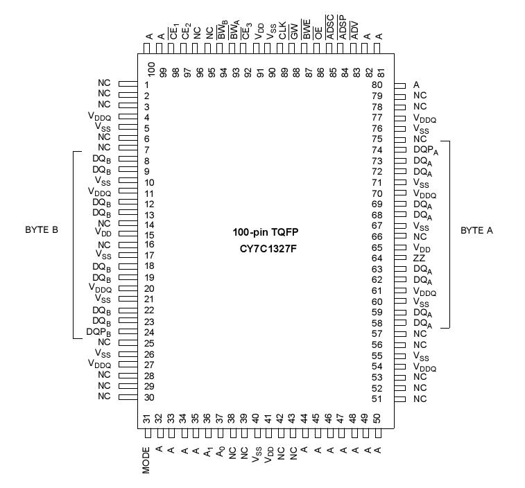
SpecificationsStorage Temperature .................................65°C to +150°C
Ambient Temperature with
Power Applied.............................................55°C to +125°C
Supply Voltage on V Relative to GND............0.5V to +4.6VDD
DC Voltage Applied to Outputs
in three-state.........................................0.5V to V + 0.5VDDQ
DC Input Voltage......................................0.5V to V + 0.5VDD
Current into Outputs (LOW).............................................20 mA
Static Discharge Voltage.............................................. > 2001V
(per MIL-STD-883, Method 3015)
Latch-up Current........................................................ > 200 mA
DescriptionThe CY7C1327F SRAM integrates 262,144 x 18 SRAM cells with advanced synchronous peripheral circuitry and a two-bit counter for internal burst operation. All synchronous inputs are gated by registers controlled by a positive-edge-triggered Clock Input (CLK). The synchronous inputs of CY7C1327F include all addresses, all data inputs, address-pipelining Chip Enable (CE ), depth-expansion Chip Enables (CE and ), Burst Control inputs ( ADSC, ADSP , ADV ), Write Enables(BW E , and ), and Global Write (GW). Asynchronous BW[A:B] inputs include the Output Enable (OE) and the ZZ pin. Addresses and chip CY7C1327F enables are registered at rising edge of clock when either Address Strobe Processor (BW [A:B] ) or Address Strobe Controller ( ADSP) are active. Subsequent
burst addresses of CY7C1327F can be internally generated as controlled by the Advance pin (ADV). Address, data inputs, and write controls are registered on-chip Bo initiate a self-timed Write cycle.This part supports Byte Write operations (see Pin Descriptions and Truth Table for further details). Write cycles can be one to two bytes wide as controlled by the byte write control inputs. GW when active LOW causes all bytes to be written. The CY7C1327F operates from a +3.3V core power supply while all outputs also operate with a +3.3V or a +2.5V supply. All inputs and outputs of CY7C1327F are JEDEC-standard JESD8-5-compatible.

 CY7C1327F Data Sheet