CY7C1305AV18

Features: • Separate independent Read and Write data ports- Supports concurrent transactions• 167 MHz Clock for high bandwidth - 2.5 ns Clock-to-Valid access time• 4-Word Burst for reducing the address bus frequency• Double Data Rate (DDR) interfaces on both Read & Writ...

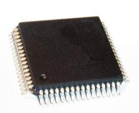
product image

CY7C1305AV18 Picture
SeekIC No. : 004319877 Detail

CY7C1305AV18: Features: • Separate independent Read and Write data ports- Supports concurrent transactions• 167 MHz Clock for high bandwidth - 2.5 ns Clock-to-Valid access time• 4-Word Burst for...

floor Price/Ceiling Price

Part Number:
CY7C1305AV18
Supply Ability:
5000

Price Break

  • Qty
  • 1~5000
  • Unit Price
  • Negotiable
  • Processing time
  • 15 Days
Total Cost: $ 0.00

SeekIC Buyer Protection PLUS - newly updated for 2013!

  • Escrow Protection.
  • Guaranteed refunds.
  • Secure payments.
  • Learn more >>

Month Sales

268 Transactions

Rating

evaluate  (4.8 stars)

Upload time: 2024/11/27

Payment Methods

All payment methods are secure and covered by SeekIC Buyer Protection PLUS.

Notice: When you place an order, your payment is made to SeekIC and not to your seller. SeekIC only pays the seller after confirming you have received your order. We will also never share your payment details with your seller.
Product Details

Description


Features:

• Separate independent Read and Write data ports
   - Supports concurrent transactions
• 167 MHz Clock for high bandwidth
   - 2.5 ns Clock-to-Valid access time
• 4-Word Burst for reducing the address bus frequency
• Double Data Rate (DDR) interfaces on both Read & Write Ports (data transferred at 333 MHz) @167 MHz
• Two input clocks (K and K) for precise DDR timing
   - SRAM uses rising edges only
• Two output clocks (C and C) accounts for clock skew and flight time mismatching
• Single multiplexed address input bus latches address inputs for both Read and Write ports
• Separate Port Selects for depth expansion
• Synchronous internally self-timed writes
• 1.8V core power supply with HSTL Inputs and Outputs
• 13 x 15 x 1.4 mm 1.0-mm pitch fBGA package, 165 ball (11x15 matrix)
• Variable drive HSTL output buffers
• Expanded HSTL output voltage (1.4V1.9V)
• JTAG Interface


Specifications

(Above which the useful life may be impaired.)
Storage Temperature ..............................65°C to +150°C
Ambient Temperature with
Power Applied .........................................55°C to +125°C
Supply Voltage on VDD
Relative to GND ............................................ 0.5V to +2.9V
DC Applied to Outputs
in High-Z State ................................... 0.5V to VDDQ + 0.5V
DC Input Voltage[11]...........................0.5V to VDDQ + 0.5V
Current into Outputs (LOW)......................................... 20 mA
Static Discharge Voltage ......................................... > 2001V
(per MIL-STD-883, Method 3015)
Latch-Up Current .................................................. > 200 mA


Description

The CY7C1305AV18/CY7C1307AV18 are 1.8V Synchronous Pipelined SRAMs equipped with QDR™ architecture. QDR architecture consists of two separate ports to access the memory array. The Read port has dedicated Data Outputs to support Read operations and the Write Port has dedicated Data Inputs to support Write operations. QDR architecture has separate data inputs and data outputs to completely eliminate the need to "turn-around" the data bus required with common I/O devices. Access to each port is accomplished through a common address bus. Addresses for Read and Write addresses are latched on alternate rising edges of the input (K) clock. Accesses to CY7C1305AV18 Read and Write ports are completely independent of one another. In order to maximize data throughput, both Read and Write ports of CY7C1305AV18 are equipped with Double Data Rate (DDR) interfaces. Each address location is associated with four 18-bit words (CY7C1305AV18) and four 36-bit words (CY7C1307AV18) that burst sequentially into or out of the device. Since data of CY7C1305AV18 can be transferred into and out of the device on every rising edge of both input clocks (K/K and
C/C) memory bandwidth is maximized while simplifying system design by eliminating bus "turn-arounds."

Depth expansion of CY7C1305AV18 is accomplished with Port Selects for each port. Port selects allow each port to operate independently.

All synchronous inputs of CY7C1305AV18 pass through input registers controlled by the K or K input clocks. All data outputs pass through output registers controlled by the C or C input clocks. Writes are conducted with on-chip synchronous self-timed write circuitry.


Customers Who Bought This Item Also Bought

Margin,quality,low-cost products with low minimum orders. Secure your online payments with SeekIC Buyer Protection.
Motors, Solenoids, Driver Boards/Modules
Prototyping Products
DE1
Connectors, Interconnects
Transformers
Sensors, Transducers
View more