Features: • Fast access times: 9 and 10 ns
• Fast clock speed: 66 and 50 MHz
• Provide high performance 2-1-1-1 access rate
• Fast OE access times: 5 and 6 ns
• Single +3.3V 5% and +10% power supply
• 5V tolerant inputs except I/Os
• Clamp diodes to VSSQ at all inputs and outputs
• Common data inputs and data outputs
• Byte Write Enable and Global Write control
• Three chip enables for depth expansion and address pipeline
• Address, data, and control registers
• Internally self-timed Write Cycle
• Burst control pins (interleaved or linear burst sequence)
• Automatic power-down for portable applications
• High-density, high-speed packages
• Low-capacitive bus loading
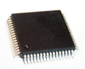
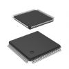
• High 30-pF output drive capability at rated access timePinout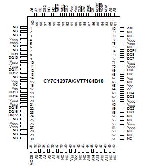 Specifications(Above which the useful life may be impaired. For user guidelines,not tested.)
Voltage on VCC Supply Relative to VSS ......... 0.5V to +4.6V
VIN ...........................................................0.5V to VCC+0.5V
Storage Temperature (plastic) ................55°C to +125°C
Junction Temperature ...............................................+125°C
Power Dissipation.......................................................... 1.4W
Short Circuit Output Current...................................... 100 mADescriptionThe Cypress Synchronous Burst SRAM family employs high-speed, low-power CMOS designs using advanced double-layer polysilicon, double-layer metal technology. Each memory cell consists of four transistors and two high-valued resistors.
The CY7C1297A/GVT7164B18 SRAM integrates 65536 * 18 SRAM cells with advanced synchronous peripheral circuitry
and a two-bit counter for internal burst operation. All synchronous inputs are gated by registers controlled by a positive-edge-triggered Clock Input (CLK). The synchronous inputs of CY7C1297A include all addresses, all data inputs,address-pipelining Chip Enable (CE), depth-expansion Chip Enables (CE2 and CE2), Burst Control inputs (ADSC, ADSP,and ADV), Write Enables (WEL, WEH, and BWE), and Global Write (GW).
Asynchronous inputs of CY7C1297A include the Output Enable (OE), Burst Mode Control (MODE), and Sleep Mode Control (ZZ). The data outputs (DQ), enabled by OE, are also asynchronous.
Addresses and chip enables are registered with either Address Status Processor (ADSP) or Address Status Controller (ADSC) input pins. Subsequent burst addresses of CY7C1297A can be internally generated as controlled by the Burst Advance pin (ADV).
Address, data inputs, and Read controls are registered on-chip to initiate self-timed Write cycle. Write cycles can be one or two bytes wide as controlled by the Read control inputs.Individual byte enables allow individual bytes to be written.WEL controls DQ1DQ8 and DQP1. WEH controls DQ9DQ16 and DQP2. WEL and WEH can be active only with BWE being LOW. GW being LOW causes all bytes to be written.
The CY7C1297A/GVT7164B18 operates from a +3.3V power supply. All inputs and outputs are TTL-compatible. The device is ideally suited for 486, Pentium®, 680 * 0, and PowerPC™ systems and for systems that benefit from a wide synchronous data bus.

 CY7C1297A Data Sheet