CY7C1219H

Features: • Registered inputs and outputs for pipelined operation• Optimal for performance (Double-Cycle deselect)- Depth expansion without wait state• 32K * 36-bit common I/O architecture• 3.3V core power supply (VDD)• 2.5V/3.3V I/O power supply (VDDQ)• Fast cl...

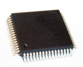
product image

CY7C1219H Picture
SeekIC No. : 004319844 Detail

CY7C1219H: Features: • Registered inputs and outputs for pipelined operation• Optimal for performance (Double-Cycle deselect)- Depth expansion without wait state• 32K * 36-bit common I/O arch...

floor Price/Ceiling Price

Part Number:
CY7C1219H
Supply Ability:
5000

Price Break

  • Qty
  • 1~5000
  • Unit Price
  • Negotiable
  • Processing time
  • 15 Days
Total Cost: $ 0.00

SeekIC Buyer Protection PLUS - newly updated for 2013!

  • Escrow Protection.
  • Guaranteed refunds.
  • Secure payments.
  • Learn more >>

Month Sales

268 Transactions

Rating

evaluate  (4.8 stars)

Upload time: 2024/7/15

Payment Methods

All payment methods are secure and covered by SeekIC Buyer Protection PLUS.

Notice: When you place an order, your payment is made to SeekIC and not to your seller. SeekIC only pays the seller after confirming you have received your order. We will also never share your payment details with your seller.
Product Details

Description


Features:

• Registered inputs and outputs for pipelined operation
• Optimal for performance (Double-Cycle deselect)
- Depth expansion without wait state
• 32K * 36-bit common I/O architecture
• 3.3V core power supply (VDD)
• 2.5V/3.3V I/O power supply (VDDQ)
• Fast clock-to-output times - 3.5 ns (for 166-MHz device)
• Provide high-performance 3-1-1-1 access rate
• User-selectable burst counter supporting Intel® Pentium® interleaved or linear burst sequences
• Separate processor and controller address strobes
• Synchronous self-timed write
• Asynchronous Output Enable
• Available in JEDEC-standard lead-free 100-Pin TQFP package
• "ZZ" Sleep Mode option


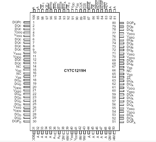
Pinout

  Connection Diagram


Specifications

(Above which the useful life may be impaired. For user guidelines,
not tested.)
Storage Temperature ................................. 65°C to + 150°
Ambient Temperature with
Power Applied.........................................55°C to + 125°C
Supply Voltage on VDD Relative to GND....... 0.5V to + 4.6V
Supply Voltage on VDDQ Relative to GND ..... 0.5V to + VDD
DC Voltage Applied to Outputs
in tri-state ......................................... 0.5V to VDDQ + 0.5V
DC Input Voltage ................................. 0.5V to VDD + 0.5V
Current into Outputs (LOW)......................................... 20 mA
Static Discharge Voltage...........................................> 2001V
(per MIL-STD-883,Method 3015)
Latch-up Current.................................................... > 200 mA


Description

The CY7C1219H SRAM integrates 32K x 36 SRAM cells with advanced synchronous peripheral circuitry and a two-bit counter for internal burst operation. All synchronous inputs are gated by registers controlled by a positive-edge-triggered Clock Input (CLK). The synchronous inputs include all addresses, all data inputs, address-pipelining Chip Enable (CE1), depth-expansion Chip Enables (CE2and CE3), Burst Control inputs (ADSC, ADSP, and ADV), Write Enables (BW[A:D], and BWE), and Global Write (GW). Asynchronous inputs include the Output Enable (OE) and the ZZ pin. Addresses and chip of CY7C1219H enables are registered at rising edge of clock when either Address Strobe Processor (ADSP) or Address Strobe Controller (ADSC) are active. Subsequent burst addresses can be internally generated as controlled by the Advance pin (ADV).

Address, data inputs, and write controls are registered on-chip to initiate a self-timed Write cycle.This part supports Byte Write operations (see Pin Descriptions and Truth Table for further details). Write cycles can be one to four bytes wide as controlled by the byte write control inputs. GW active LOW causes all bytes to be written. CY7C1219H incorporates an additional pipelined enable register which delays turning off the output buffers an additional cycle when a deselect is executed.This feature allows depth expansion without penalizing system performance.

The CY7C1219H operates from a +3.3V core power supply while all outputs operate with either a +2.5V or +3.3V supply. All inputs and outputs are JEDEC-standard JESD8-5-compatible.


Customers Who Bought This Item Also Bought

Margin,quality,low-cost products with low minimum orders. Secure your online payments with SeekIC Buyer Protection.
Sensors, Transducers
Static Control, ESD, Clean Room Products
Undefined Category
LED Products
Discrete Semiconductor Products
Boxes, Enclosures, Racks
View more