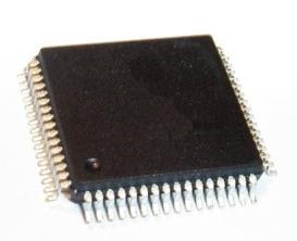
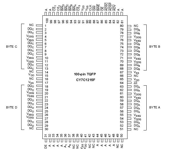
Features: Registered inputs and outputs for pipelined operation32K * 32 common I/O architecture 3.3V core power supply3.3V I/O operationFast clock-to-output times - 3.5ns (for 166-MHz device) - 4.0 ns (for 133-MHz device)Provide high-performance 3-1-1-1 access rateUser-selectable burst counter su...
CY7C1215F: Features: Registered inputs and outputs for pipelined operation32K * 32 common I/O architecture 3.3V core power supply3.3V I/O operationFast clock-to-output times - 3.5ns (for 166-MHz device) - 4.0...
SeekIC Buyer Protection PLUS - newly updated for 2013!
268 Transactions
All payment methods are secure and covered by SeekIC Buyer Protection PLUS.
The CY7C1215F SRAM integrates 32,768 x 32 SRAM cellswith advanced synchronous peripheral circuitry and a two-bitcounter for internal burst operation. All synchronous inputs aregated by registers controlled by a positive-edge-triggeredClock Input (CLK). The synchronous inputs include alladdresses, all data inputs, address-pipelining Chip Enable(CE1)CY7C1215F, depth-expansion Chip Enables (CE2andCE3), BurstControl inputs (ADSC ,ADSP , and ADV ), Write Enables(BW [A:D], andBWE ), and Global Write (GW ). Asynchronousinputs include the Output Enable (OE ) and the ZZ pin.
Addresses and chip enables of CY7C1215F are registered at rising edge ofclock when either Address Strobe Processor (ADSP ) orAddress Strobe Controller (ADSC ) are active. Subsequentburst addresses can be internally generated as controlled by
the Advance pin (ADV ).
Address, data inputs, and write controls are registered on-chipto initiate a self-timed Write cycle.This part supports Byte Writeoperations (see Pin Descriptions and Truth Table for furtherdetails). Write cycles of CY7C1215F can be one to four bytes wide ascontrolled by the Byte Write control inputs. GW when activeLOW causes all bytes to be written.
The CY7C1215F operates from a +3.3V core power supplywhile all outputs may operate with a +3.3V supply. All inputsand outputs are JEDEC-standard JESD8-5-compatible.