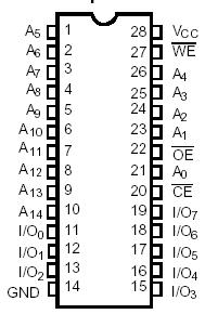
Features: • High speed -15 ns tAA• Single 5V power supply with 3.3V-compatible I/Os -VOH max. of 3.435V• Fast tDOEPinoutSpecifications(Above which the useful life may be impaired. For user guidelines, not tested.)Storage Temperature ............................. 65°C to +150°CAmb...
CY7C1199: Features: • High speed -15 ns tAA• Single 5V power supply with 3.3V-compatible I/Os -VOH max. of 3.435V• Fast tDOEPinoutSpecifications(Above which the useful life may be impaired. ...
SeekIC Buyer Protection PLUS - newly updated for 2013!
268 Transactions
All payment methods are secure and covered by SeekIC Buyer Protection PLUS.
The CY7C1199 is a high-performance CMOS static RAM organized as 32,768 words by 8 bits. The device operates with a single 5V power supply but internally clamps the output voltage level to a maximum of 3.435V. The internal clamps of CY7C1199 allow the CY7C1199 to interface to 3.3V processors (such as the Pentium™ processor) without buffers or level translators. Easy memory expansion of CY7C1199 is provided by an active LOW chip enable (CE) and active LOW output enable (OE) and three-state drivers. This device has an automatic power-down feature, that reduces the power consumption significantly when deselected.
An active LOW write enable signal (WE)CY7C1199 controls the writing/ reading operation of the memory. When CE and WE inputs are both LOW, data on the eight data input/output pins (I/O0 through I/O7) is written into the memory location addressed by the address present on the address pins (A0 through A14).
Reading CY7C1199 is accomplished by selecting the device and enabling the outputs, CE and OE active LOW, while WE remains inactive or HIGH. Under these conditions, the contents of the location addressed by the information on address pins is present on the eight data input/output pins.
The input/output pins remain in a high-impedance state unless the chip is selected, outputs of CY7C1199 are enabled, and write enable (WE) is HIGH.
The CY7C1199 is available in standard 300-mil-wide SOJ packages.