Features: •High speed-tAA = 8, 10, 12 ns
•Low active power-1080 mW (max.)
•Operating voltages of 3.3 ± 0.3V
•2.0V data retention
•Automatic power-down when deselected
•TTL-compatible inputs and outputs
•Easy memory expansion with CE1 and CE2 featuresPinout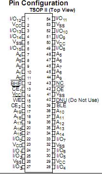 Specifications
(Applications) (Above which the useful life may be impaired. For user guide-
lines, not tested.)
Storage Temperature .................................65°C to +150°C
Ambient Temperature with
Power Applied.............................................55°C to +125°C
Supply Voltage on VCC to Relative GND[1]....0.5V to +4.6V
DC Voltage Applied to Outputs
in High-Z State[1]....................................0.5V to VCC + 0.5V
DescriptionWriting to CY7C1061AV33 is accomplished by enabling the chip(CE1 LOW and CE2 HIGH) while forcing the Write Enable(WE) input LOW. If Byte Low Enable (BLE) is LOW, then datafrom I/O pins (I/O through I/O7), is written into the locationspecified on the address pins (A0 through A19). If Byte HighEnable (BHE) is LOW, then data of CY7C1061AV33 from I/O pins (I/O8 throughI/O15) is written into the location specified on the address pins(A0 through A19).
Reading from the device is accomplished by enabling the chipby taking CE1LOW and CE2 HIGH while forcing the OutputEnable (OE) LOW and the Write Enable (WE) HIGH. If ByteLow Enable (BLE) is LOW, then data of CY7C1061AV33 from the memory locationspecified by the address pins will appear on I/O0 to I/O7. If Byte High Enable (BHE) is LOW, then data from memory will appearon I/O8 to I/O15. See the truth table at the back of this datasheet for a complete description of Read and Write modes.
The input/output pins (I/O0 through I/O15) are placed in ahigh-impedance state when CY7C1061AV33 is deselected (CE1HIGH/CE2 LOW), the outputs are disabled (OE HIGH), theBHE and BLE are disabled (BHE, BLE HIGH), or during aWrite operation (CE1LOW, CE2HIGH, and WE LOW).
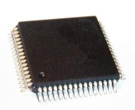
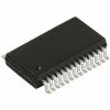
The CY7C1061AV33 is available in a 54-pin TSOP II packagewith center power and ground (revolutionary) pinout, and a48-ball fine-pitch ball grid array (FBGA) package.

 CY7C1061AV33 Data Sheet