Features: High speed
-t AA = 10 ns
Low active power for 10 ns speed
-540 mW (max.)
Low CMOS standby power (L version)
-1.8 mW (max.)
2.0V Data Retention (400 W at 2.0V retention)
Automatic power-down when deselected
TTL-compatible inputs and outputs
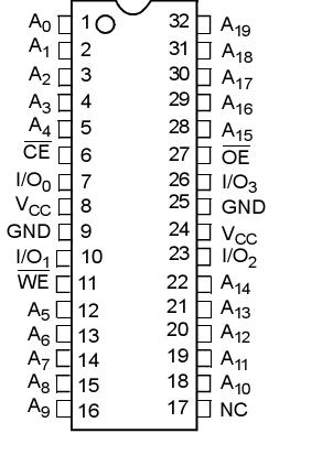
Easy memory expansion with CE and OE featuresPinout Specifications
Storage Temperature .................................65°C to +150°C
Ambient Temperature with
Power Applied.............................................55°C to +125°C
Supply Voltage on V to Relative GND[1] ...........0.5V to +4.6V
DC Voltage Applied to Outputs
in High Z State [1].....................................0.5V to V CC + 0.5V
DC Input Voltage[1]...................................0.5V to VCC + 0.5V
Current into Outputs (LOW) ..............................................20 mA
Static Discharge Voltage..................................................>2001V
(per MIL-STD-883, Method 3015)
Latch-Up Current............................................................>200 mA
DescriptionThe CY7C1046BV33 is a high-performance CMOS static RAM organized as 1,048,576 words by 4 bits. Easy memoryexpansion is provided by an active LOW Chip Enable (CE ), an active LOW Output Enable (OE), and three-state drivers. Writ- ing to the device is accomplished by taking Chip Enable (CE ) and Write Enable (WE) inputs LOW. Data on the four I/O pins(I/O3 through I/O ) is then written into the location specified on the address pins (A 0 through A19 ).
Reading from CY7C1046BV33 is accomplished by taking Chip Enable (CE ) and Output Enable (OE) LOW while forcing Write Enable (WE) HIGH. Under these conditions, the contents of the memory location specified by the address pins will appear on the I/O pins. The four input/output pins (I/O through I/O ) are placed in a high-impedance state when CY7C1046BV33 is deselected (CE HIGH), the outputs are disabled (OE HIGH), or during a write operation (CE LOW, and WE LOW). The CY7C1046BV33 is available in a standard 400-mil-wide 32-pin SOJ package with center power and ground (revolution- ary) pinout.

 CY7C1046BV33 Data Sheet


