Features: Pin equivalent to CY7C1041BV33
High speed
-tAA = 10 ns
Low active power
-324 mW (max.)
2.0V data retention
Automatic power-down when deselected
TTL-compatible inputs and outputs
Easy memory expansion with CE and OE featuresPinout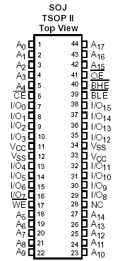 Specifications
(Above which the useful life may be impaired. For user guide-lines, not tested.)
Storage Temperature .................................65°C to +150°C
Ambient Temperature with
Power Applied.............................................55°C to +125°C
Supply Voltage on VCC to Relative GND[2]....0.5V to +4.6V
DC Voltage Applied to Outputsin
High-Z State[2]....................................0.5V to VCC + 0.5V
DescriptionThe CY7C1041CV33 is a high-performance CMOS Static RAM organized as 262,144 words by 16 bits.
Writing to the device is accomplished by taking Chip Enable (CE) and Write Enable (WE) inputs LOW. If Byte LOW Enable (BLE) is LOW, then data from I/O pins (I/O0I/O7), is written into the location specified on the address pins (A0A17). If Byte HIGH Enable (BHE) is LOW, then data from I/O pins (I/O8I/O15) is written into the location specified on the address pins (A0A17).
Reading from CY7C1041CV33 is accomplished by taking Chip Enable (CE) and Output Enable (OE) LOW while forcing the
Write Enable (WE) HIGH. If Byte LOW Enable (BLE) is LOW,then data from the memory location specified by the address pins will appear on I/O0 I/O7. If Byte HIGH Enable (BHE) is LOW, then data of CY7C1041CV33 from memory will appear on I/O8 to I/O15. See the truth table at the back of this data sheet for a complete description of Read and Write modes.
The input/output pins (I/O0I/O15) are placed in a high-impedance state when the device is deselected (CE
HIGH), the outputs are disabled (OE HIGH), the BHE and BLE are disabled (BHE , BLE HIGH), or during a Write operation
(CE LOW, and WE LOW).
The CY7C1041CV33 is available in a standard 44-pin 400-mil-wide body width SOJ and 44-pin TSOP II package with center power and ground (revolutionary) pinout, as well as a 48-ball fine-pitch ball grid array (FBGA) package.

 CY7C1041CV33 Data Sheet