Features: •3.3V operation (3.0V3.6V)
•High speed-tAA = 10/12/15 ns
•CMOS for optimum speed/power
•Low Active Power (L version)-576 mW (max.)
•Low CMOS Standby Power (L version)-1.80 mW (max.)
•Automatic power-down when deselected
•Independent control of upper and lower bits
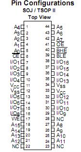
•Available in 44-pin TSOP II and 400-mil SOJ
•Available in a 48-Ball Mini BGA packagePinout Specifications
(Above which the useful life may be impaired. For user guide-lines, not tested.)
Storage Temperature .......................................................65°C to +150°C
Ambient Temperature with
Power Applied...................................................................55°C to +125°C
Supply Voltage on VCC to Relative GND[2]..............................0.5V to +4.6V
DC Voltage Applied to Outputs
in High Z State[2]..............................................................0.5V to VCC+0.5V
DC Input Voltage[2]..........................................................0.5V to VCC+0.5V
Current into Outputs (LOW)........................................20 mA
Static Discharge Voltage............................................>2001V
(per MIL-STD-883, Method 3015)
Latch-Up Current.....................................................>200 mA
DescriptionThe CY7C1021BV is a high-performance CMOS static RAM organized as 65,536 words by 16 bits. This device has an au-tomatic power-down feature that significantly reducespowerconsumption when deselected.
Writing to CY7C1021BV33 is accomplished by taking Chip Enable(CE) and Write Enable (WE) inputs LOW. If Byte Low Enable(BLE) is LOW, then data from I/O pins (I/O1through I/O8), is written into the location specified on the address pins (A0through A15). If Byte High Enable (BHE) is LOW, then datafrom I/O pins (I/O9through I/O16) CY7C1021BV33 is written into the locationspecified on the address pins (A0through A15).
Reading from CY7C1021BV33 is accomplished by taking Chip En-able (CE) and Output Enable (OE) LOW while forcing the WriteEnable (WE) HIGH. If Byte Low Enable (BLE) is LOW, thendata from the memory location specified by the address pinswill appear on I/O1 to I/O8. If Byte High Enable (BHE) is LOW,then data from memory CY7C1021BV33 will appear on I/O9 to I/O16.See thetruth table at the back of this data sheet for a complete descrip-tion of read and write modes.
The input/output pins (I/O1through I/O16(CEHIGH)CY7C1021BV33, the outputs are disabled (OE HIGH), the BHEBLEare disabled (BHE, BLEtion (CE LOW, and WE LOW).
The CY7C1021BV is available in 400-mil-wide SOJ, standard44-pin TSOP Type II, and 48-ball mini BGA packages.

 CY7C1021BV33 Data Sheet


