Features: • High speed
-tAA = 10 ns
• Low active power
-1017 mW (max., 12 ns)
• Low CMOS standby power
-55 mW (max.), 4 mW (Low power version)
• 2.0V Data Retention (Low power version)
• Automatic power-down when deselected
• TTL-compatible inputs and outputs
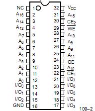
• Easy memory expansion with CE1, CE2, and OE optionsPinout
SpecificationsStorage Temperature .........................................................65°C to +150°C
Ambient Temperature with
Power Applied..................................................................... 55°C to +125°C
Supply Voltage on VCC to Relative GND[1].... ............................0.5V to +7.0V
DC Voltage Applied to Outputs in High Z State[1]..............0.5V to VCC + 0.5V
DC Input Voltage[1]...........................................................0.5V to VCC + 0.5V
Current into Outputs (LOW) .....................................................................20 mA
Static Discharge Voltage ....................................................................... >2001V
(per MIL-STD-883, Method 3015)
Latch-Up Current ................................................................................. >200 mADescriptionThe CY7C109 / CY7C1009 is a high-performance CMOS stat-ic RAM organized as 131,072 words by 8 bits. Easy memory expansion is provided by an active LOW chip enable (CE1), anactive HIGH chip enable (CE2), an active LOW output enable (OE), and three-state drivers. Writing to CY7C1009 is accom-plished by taking chip enable one (CE1) and write enable (WE) inputs LOW and chip enable two (CE2) input HIGH. Data on the eight I/O pins (I/O0 through I/O7) is then written into the location specified on the address pins (A0 through A16).
Reading from CY7C1009 is accomplished by taking chip en-able one (CE1) and output enable (OE) LOW while forcing
write enable (WE) and chip enable two (CE2) HIGH. Under these conditions, the contents of the memory location speci-fied by the address pins will appear on the I/O pins.
The eight input/output pins (I/O0 through I/O7) are placed in a high-impedance state when CY7C1009 is deselected (CE1 HIGH or CE2 LOW), the outputs are disabled (OE HIGH), or during a write operation (CE1 LOW, CE2 HIGH, and WE LOW).
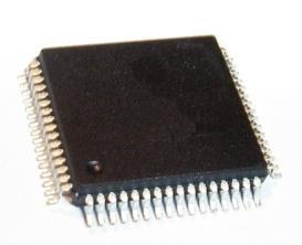
The CY7C109 is available in standard 400-mil-wide SOJ and 32-pin TSOP type I packages. The CY7C1009 is available in a 300-mil-wide SOJ package. The CY7C1009 and CY7C109 are functionally equivalent in all other respects.

 CY7C1009 Data Sheet


