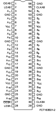
Features: * Low power, pin-compatible replacement for LCX and LPT families
* 5V tolerant inputs and outputs
* 24 mA balanced drive outputs
* Power-off disable outputs permits live insertion
* Edge-rate control circuitry for reduced noise
* FCT-C speed at 4.6 ns
* Latch-upperformanceexceedsJEDECstandardno.17
* ESD > 2000V per MIL-STD-883D, Method 3015
* Typical output skew < 250ps
* Industrial temperature range of 40?C to +85?C
* TSSOP (19.6-mil pitch) or SSOP (25-mil pitch)
* TypicalVolp (groundbounce)performanceexceedsMil Std 883D
* VCC = 2.7V to 3.6V CY74FCT163501 Features:
* Balanced output drivers: 24 mA
* Reduced system switching noise
* Typical VOLP (ground bounce) <0.6V at VCC = 3.3V,TA = 25?CPinout Specifications(Above which the useful life may be impaired. For user guidelines, not tested.)
Storage Temperature ....................................- 55 C to +125 C
Ambient Temperature with
Power Applied.................................................- 55 C to +125 C
DC Input Voltage...............................................- 0.5V to +7.0V
DC Output Voltage............................................- 0.5V to +7.0V
DC Output Current
(Maximum Sink Current/Pin).............................- 60 to +120 mA
Power Dissipation..............................................................1.0W
Static Discharge Voltage................................................>2001V
(per MIL-STD-883, Method 3015)DescriptionThese 18-bit universal bus transceivers of CY74FCT163501 can be operated in transparent, latched or clock modes by combining D-type latches and D-type flip-flops. Data flow in each direction is controlled by output enable (OEAB and OEBA), latch enable (LEABandLEBA),andclockinputs(CLKABandCLKBA).For A-to-B data flow, the CY74FCT163501 operates in transparent mode when LEAB is HIGH. When LEAB is LOW, the A data is latchedifCLKABisheldataHIGHorLOWlogiclevel.IfLEAB is LOW, the A bus data is stored in the latch/flip-flop on the LOW-to-HIGHtransitionofCLKAB.OEABperformstheoutput enable function on the B port. Data flow from B-to-A is similar to that of A-to-B and is controlled by OEBA, LEBA, and CLKBA. The output buffers of CY74FCT163501 are designed with a power-off disable feature to allow live insertion of boards.
THE CY74FCT163501 has 24-mA balanced output drivers with current limiting resistors in the outputs. This reduces the need for external terminating resistors, as well as provides for minimal undershoot and reduced ground bounce. TheCY74FCT163501 is ideal for driving transmission lines.
The CY74FCT163H501 is a24-mA balanced output part, that has "bus hold" on the data inputs. The CY74FCT163501 retains the input's last state whenever the input goes to high impedance. This eliminates the need for pull-up/down resistors and prevents floating inputs.

 CY74FCT163501 Data Sheet


