Features: • 4.5V5.5V operation• Low active power -Typical active current: 2.5 mA @ f = 1 MHz -Typical active current: 12.5 mA @ f = fmax• Low standby current• Automatic power-down when deselected• TTL-compatible inputs and outputs• Easy memory expansion withCE a...
CY62148B: Features: • 4.5V5.5V operation• Low active power -Typical active current: 2.5 mA @ f = 1 MHz -Typical active current: 12.5 mA @ f = fmax• Low standby current• Automatic power...
SeekIC Buyer Protection PLUS - newly updated for 2013!
268 Transactions
All payment methods are secure and covered by SeekIC Buyer Protection PLUS.
Features: • Very high speed: 45 ns• Wide voltage range: 2.2V to 3.6V• Pin compat...
Storage Temperature ....................................................................65°C to +150°C
Ambient Temperature with Power Applied..................................... 55°C to +125°C
Supply Voltage on VCC to Relative GND ............................................ 0.5V to +7.0V
DC Voltage Applied to Outputs in High Z State[1] ......................0.5V to VCC +0.5V
DC Input Voltage[1] ....................................................................0.5V to VCC +0.5V
Current into Outputs (LOW) ............................................................................ 20 mA
Static Discharge Voltage....................................................................................2001V
(per MIL-STD-883, Method 3015) Latch-Up Current...................................... >200 mA
The CY62148B is a high-performance CMOS static RAM organized as 512K words by 8 bits. Easy memory expansion is provided by an active LOW Chip Enable (CE), an active LOW Output Enable (OE), and three-state drivers. CY62148B has an automatic power-down feature that reduces power consumption by more than 99% when deselected.
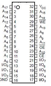
Writing to the CY62148B is accomplished by taking Chip Enable (CE) and Write Enable (WE) inputs LOW. Data on the eight I/O pins (I/O0 through I/O7) is then written into the location specified on the address pins (A0 through A18).
Reading from the CY62148B is accomplished by taking Chip Enable (CE) and Output Enable (OE) LOW while forcing Write Enable (WE) HIGH for read. Under these conditions, the contents of the memory location specified by the address pins will appear on the I/O pins.
The eight input/output pins of CY62148B (I/O0 through I/O7) are placed in a high-impedance state when the device is deselected (CE HIGH), the outputs are disabled (OE HIGH), or during a write operation (CE LOW, and WE LOW).
The CY62148B is available in a standard 32-pin 450-mil-wide body width SOIC, 32-pin TSOP II, and 32-pin Reverse TSOP II packages.