CY62147EV30

Features: • Very high speed: 45 ns• Temperature ranges - Industrial: 40 to +85 - Automotive-A: 40 to +85 - Automotive-E: 40 to +125• Wide voltage range: 2.20V3.60V• Pin compatible with CY62147DV30• Ultra low standby power - Typical standby current: 1 A - Maximum stand...

product image

CY62147EV30 Picture
SeekIC No. : 004319434 Detail

CY62147EV30: Features: • Very high speed: 45 ns• Temperature ranges - Industrial: 40 to +85 - Automotive-A: 40 to +85 - Automotive-E: 40 to +125• Wide voltage range: 2.20V3.60V• Pin compa...

floor Price/Ceiling Price

Part Number:
CY62147EV30
Supply Ability:
5000

Price Break

  • Qty
  • 1~5000
  • Unit Price
  • Negotiable
  • Processing time
  • 15 Days
Total Cost: $ 0.00

SeekIC Buyer Protection PLUS - newly updated for 2013!

  • Escrow Protection.
  • Guaranteed refunds.
  • Secure payments.
  • Learn more >>

Month Sales

268 Transactions

Rating

evaluate  (4.8 stars)

Upload time: 2024/11/23

Payment Methods

All payment methods are secure and covered by SeekIC Buyer Protection PLUS.

Notice: When you place an order, your payment is made to SeekIC and not to your seller. SeekIC only pays the seller after confirming you have received your order. We will also never share your payment details with your seller.
Product Details

Description


Features:

• Very high speed: 45 ns
• Temperature ranges
   - Industrial: 40 to +85
   - Automotive-A: 40 to +85
   - Automotive-E: 40 to +125
• Wide voltage range: 2.20V3.60V
• Pin compatible with CY62147DV30
• Ultra low standby power
   - Typical standby current: 1 A
   - Maximum standby current: 7 A (Industrial)
• Ultra low active power
   - Typical active current: 2 mA @ f = 1 MHz
• Easy memory expansion with CE and OE features
• Automatic power down when deselected
• CMOS for optimum speed and power
• Offered in Pb-free 48-ball VFBGA and 44-pin TSOPII packages
• Byte power down feature


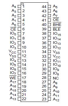
Pinout

  Connection Diagram


Specifications

Exceeding the maximum ratings may shorten the battery life of the device. User guidelines are not tested.
Storage Temperature ................................65°C to + 150°C
Ambient Temperature with
Power Applied ...........................................55°C to + 125°C
Supply Voltage to Ground
Potential .............................. 0.3V to + 3.9V (VCCmax + 0.3V)
DC Voltage Applied to Outputs
in High-Z State [5, 6] ................0.3V to 3.9V (VCCmax + 0.3V)
DC Input Voltage [5, 6] .............0.3V to 3.9V (VCCmax + 0.3V)
Output Current into Outputs (LOW) ............................... 20 mA
Static Discharge Voltage .............................................. >2001V
(MIL-STD-883, Method 3015)
Latch up Current......................................................... >200 mA


Description

The CY62147EV30 is a high performance CMOS static RAM organized as 256K words by 16 bits. This device features advanced circuit design to provide ultra low active current. This is ideal for providing More Battery Life™ (MoBL®) in portable applications such as cellular telephones. The CY62147EV30 also has an automatic power down feature that significantly reduces power consumption when addresses are not toggling. Placing the CY62147EV30 into standby mode reduces power consumption by more than 99% when deselected (CE HIGH or both BLE and BHE are HIGH). The input and output pins (IO0 through IO15) are placed in a high impedance state when:
• Deselected (CE HIGH)
• Outputs are disabled (OE HIGH)
• Both Byte High Enable and Byte Low Enable are disabled (BHEBLE HIGH)
• Write operation is active (CE LOW and WE LOW)

To write to the CY62147EV30, take Chip Enable (CE) and Write Enable (WE) inputs LOW. If Byte Low Enable (BLE) is LOW, then data from IO pins (IO0 through IO7) is written into the location specified on the address pins (A0 through A17). If Byte High Enable (BHE) is LOW, then data from IO pins of CY62147EV30 (IO8 through IO15) is written into the location specified on the address pins (A0 through A17).

To read from the CY62147EV30, take Chip Enable (CE) and Output Enable (OE) LOW while forcing the Write Enable (WE) HIGH. If Byte Low Enable (BLE) is LOW, then data from the memory location specified by the address pins appear on IO0 to IO7. If Byte High Enable (BHE) is LOW, then data of CY62147EV30 from memory appears on IO8  to IO15. See the "Truth Table" on page 9 for a complete description of read and write modes.


Customers Who Bought This Item Also Bought

Margin,quality,low-cost products with low minimum orders. Secure your online payments with SeekIC Buyer Protection.
Cables, Wires - Management
Motors, Solenoids, Driver Boards/Modules
Batteries, Chargers, Holders
Transformers
Tapes, Adhesives
803
View more