Features: • High Speed
-55 ns and 70 ns availability
• Low voltage range:
-CY62137CV18: 1.65V−1.95V
• Pin Compatible w/ CY62137V18/BV18
• Ultra-low active power
-Typical Active Current: 0.5 mA @ f = 1 MHz
-Typical Active Current: 1.5 mA @ f = fmax (70 ns speed)
• Low standby power
• Easy memory expansion with CE and OE features
• Automatic power-down when deselected
• CMOS for optimum speed/powerPinout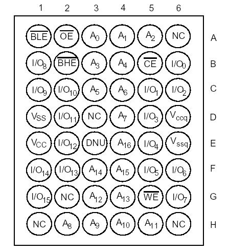 SpecificationsStorage Temperature .......................................................................... −65°C to +150°C
Ambient Temperature with Power Applied.............................................−55°C to +125°C
Supply Voltage to Ground Potential .............................................................−0.2V to +2.4V
in High Z State[3] ............................................................................... −0.2V to VCC + 0.2V
DC Input Voltage[3]............................................................................ −0.2V to VCC + 0.2V
Output Current into Outputs (LOW).......................................................................... 20 mA
Static Discharge Voltage ......................................................................................... >2001V
(per MIL-STD-883, Method 3015) Latch-Up Current............................................... >200 mADescriptionThe CY62137CV18 is a high-performance CMOS static RAM organized as 128K words by 16 bits. This device features advanced circuit design to provide ultra-low active current. This is ideal for providing More Battery Life™ (MoBL™) in portable applications such as cellular telephones. The device also has an automatic power-down feature that significantly reduces power consumption by 99% when addresses are not toggling.
The CY62137CV18 can also be put into standby mode when deselected (CE HIGH or both BLE and BHE are HIGH). The input/output pins (I/O0 through I/O15) are placed in a high-impedance state when: deselected (CE HIGH), outputs are disabled (OE HIGH), both Byte High Enable and Byte Low Enable are disabled (BHE, BLE HIGH), or during a write operation (CE LOW, and WE LOW).
Writing to the device is accomplished by taking Chip Enable (CE ) and Write Enable (WE ) inputs LOW. If Byte Low Enable (BLE ) is LOW, then data from I/O pins (I/O0 through I/O7), is written into the location specified on the address pins (A0 through A16). If Byte High Enable (BHE) is LOW, then data from I/O pins (I/O8 through I/O15) is written into the location specified on the address pins (A0 through A16).
Reading from the CY62137CV18 is accomplished by taking Chip Enable (CE ) and Output Enable (CE ) LOW while forcing the Write Enable (WE) HIGH. If Byte Low Enable (BLE ) is LOW, then data from the memory location specified by the address pins will appear on I/O0 to I/O7. If Byte High Enable (BHE) is LOW, then data from memory will appear on I/O8 to I/O15. See the Truth Table at the back of this data sheet for a complete description of read and write modes.
The CY62137CV18 is available in a 48-ball FBGA package.

 CY62137CV18 Data Sheet