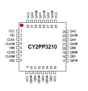
Features: • Dual sets of five ECL/PECL differential outputs• Two ECL/PECL differential inputs• Hot-swappable/-insertable• 50 ps output-to-output skew• 150 ps device-to-device skew• 500 ps propagation delay (typical)• 0.8 ps RMS period jitter (max.)• ...
CY2PP3210: Features: • Dual sets of five ECL/PECL differential outputs• Two ECL/PECL differential inputs• Hot-swappable/-insertable• 50 ps output-to-output skew• 150 ps device-to-...
SeekIC Buyer Protection PLUS - newly updated for 2013!
268 Transactions
All payment methods are secure and covered by SeekIC Buyer Protection PLUS.
Parameter |
Description | Condition |
Min. |
Max. |
Unit |
VCC |
Positive Supply Voltage | Non-Functional |
0.3 |
4.6 |
V |
VEE |
Negative Supply Voltage | Non-Functional |
-4.6 |
0.3 |
V |
TS |
Temperature, Storage | Non-Functional |
65 |
+150 |
°C |
TJ |
Temperature, Junction | Non-Functional |
150 |
°C | |
ESDh |
ESD Protection | Human Body Model |
2000 |
V | |
MSL |
Moisture Sensitivity Level |
3 |
N.A. | ||
Gate Count |
Total Number of Used Gates | Assembled Die |
50 |
gates |
The CY2PP3210 is a low-skew, low propagation delay dual 1-to-5 differential fanout buffer targeted to meet the requirements of high-performance clock and data distribution applications.
The device is implemented on SiGe technology and has a fully differential internal architecture that is optimized to achieve low signal skews at operating frequencies of up to 1.5 GHz.
The device features two differential input paths that are differential internally. The CY2PP3210 may function not only as a differential clock buffer but also as a signal-level translator and fanout distributing a single-ended signal. An external bias pin, VBB, is provided for this purpose. In such an application, the VBB pin should be connected to either one of the CLKA# or CLKB# inputs and bypassed to ground via a 0.01-F capacitor. Traditionally, in ECL, it is used to provide the reference level to a receiving single-ended input that might have a differential bias point.
Since the CY2PP3210 introduces negligible jitter to the timing budget, it is the ideal choice for distributing high frequency, high precision clocks across back-planes and boards in communication systems. Furthermore, advanced circuit design schemes, such as internal temperature compensation, ensure that the CY2PP3210 delivers consistent performance over various platforms.