Features: •Output frequency range: 8.33 MHz to 200 MHz
•Input frequency range: 6.25 MHz to 125 MHz
•2.5V or 3.3V operation
•Split 2.5V/3.3V outputs
•±2% max Output duty cycle variation
•12 Clock outputs: drive up to 24 clock lines
•One feedback output
•Three reference clock inputs: LVPECL or LVCMOS
•300-ps max output-output skew
•Phase-locked loop (PLL) bypass mode
•Spread Aware™
•Output enable/disable
•Pin-compatible with MPC9773 and MPC973
•Industrial temperature range: 40to +85
•52-pin 1.0-mm TQFP package
Pinout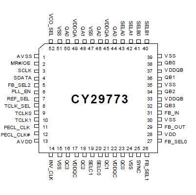 Specifications
| Parameter |
Description |
Condition |
Min. |
Max. |
Unit |
| VDD |
DC Supply Voltage |
|
0.3 |
5.5 |
V |
| VDD |
DC Operating Voltage |
Functional |
2.375 |
3.465 |
V |
| VIN |
DC Input Voltage |
Relative to VSS |
0.3 |
VDD + 0.3 |
V |
| VOUT |
DC Output Voltage |
Relative to VSS |
0.3 |
VDD + 0.3 |
V |
| VTT |
Output termination Voltage |
|
|
VDD ÷ 2 |
V |
| LU |
Latch-up Immunity |
Functional |
200 |
|
mA |
| RPS |
Power Supply Ripple |
Ripple Frequency < 100 kHz |
|
150 |
mVp-p |
| TS |
Temperature, Storage |
Non-functional |
65 |
+150 |
|
| TA |
Temperature, Operating Ambient |
Functional |
40 |
+85 |
|
| TJ |
Temperature, Junction |
Functional |
|
+150 |
|
| ØJC |
Dissipation, Junction to Case |
Functional |
|
23 |
/W |
| ØJA |
Dissipation, Junction to Ambient |
Functional |
|
55 |
/W |
| ESDH |
ESD Protection (Human Body Model) |
|
2000 |
V |
| FIT |
Failure in Time |
Manufacturing test |
10 |
ppm |
DescriptionThe CY29773 is a low-voltage high-performance 200-MHz PLL-based zero delay buffer designed for high speed clock distribution applications.
The CY29773 features one LVPECL and two LVCMOS reference clock inputs and provides 12 outputs partitioned in three banks of four outputs each. Each bank divides the VCO output per SEL(A:C) settings (see Table 2. Function Table (Configuration Controls)). These dividers allow output-to-input ratios of 8:1, 6:1, 5:1, 4:1, 3:1, 8:3, 5:2, 2:1, 5:3, 3:2, 4:3, 5:4, 1:1, and 5:6. Each LVCMOS-compatible output can drive 50 series- or parallel-terminated transmission lines. For series-terminated transmission lines, each output can drive one or two traces, giving the device an effective fanout of 1:24.
The PLL is ensured stable, given that the VCO is configured to run between 200 MHz to 500 MHz. This allows a wide range of output frequencies, from 8 MHz to 200 MHz. For normal operation, the external feedback input FB_IN is connected to the feedback output FB_OUT. The internal VCO is running at multiples of the input reference clock set by the feedback divider (see Table 1. Frequency Table).
When PLL_EN is LOW, PLL is bypassed and the reference clock directly feeds the output dividers. This mode is fully static and the minimum input clock frequency specification does not
apply.

 CY29773 Data Sheet


