CY23S08

Features: • Zero input-output propagation delay, adjustable by capacitive load on FBK input• Multiple configurations, see Table 2• Multiple low-skew outputs- 45ps typical output-output skew(1)- Two banks of four outputs, three-stateable by two select inputs• 10-MHz to 133-M...

product image

CY23S08 Picture
SeekIC No. : 004319166 Detail

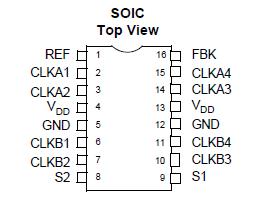
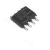
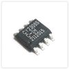
CY23S08: Features: • Zero input-output propagation delay, adjustable by capacitive load on FBK input• Multiple configurations, see Table 2• Multiple low-skew outputs- 45ps typical output-ou...
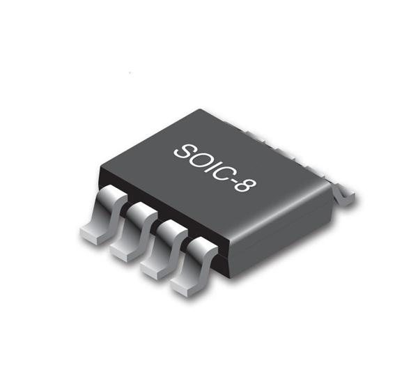
floor Price/Ceiling Price

Part Number:
CY23S08
Supply Ability:
5000

Price Break

  • Qty
  • 1~5000
  • Unit Price
  • Negotiable
  • Processing time
  • 15 Days
Total Cost: $ 0.00

SeekIC Buyer Protection PLUS - newly updated for 2013!

  • Escrow Protection.
  • Guaranteed refunds.
  • Secure payments.
  • Learn more >>

Month Sales

268 Transactions

Rating

evaluate  (4.8 stars)

Upload time: 2024/6/8

Payment Methods

All payment methods are secure and covered by SeekIC Buyer Protection PLUS.

Notice: When you place an order, your payment is made to SeekIC and not to your seller. SeekIC only pays the seller after confirming you have received your order. We will also never share your payment details with your seller.
Product Details

Description


Features:

• Zero input-output propagation delay, adjustable by capacitive load on FBK input
• Multiple configurations, see Table 2
• Multiple low-skew outputs
- 45ps typical output-output skew(1)
- Two banks of four outputs, three-stateable by two select inputs
• 10-MHz to 133-MHz operating range
• 65ps typical cycle-cycle jitter (1, 1H)
• Advanced 0.65 CMOS technology
• Space-saving 16-pin 150-mil SOIC/TSSOP packages
• 3.3V operation
• Spread Aware™


Pinout

  Connection Diagram


Specifications

Supply Voltage to Ground Potential ............... 0.5V to +7.0V
DC Input Voltage (Except Ref)...............0.5V to VDD + 0.5V
DC Input Voltage REF............................................0.5 to 7V
Storage Temperature ................................. 65°C to +150°C
Max. Soldering Temperature (10 sec.) ....................... 260°C
Junction Temperature................................................. 150°C
Static Discharge Voltage
(per MIL-STD-883, Method 3015) ............................. >2000V


Description

The CY23S08 is a 3.3V zero delay buffer designed to distribute high-speed clocks in PC, workstation, datacom, telecom, and other high-performance applications.

The part has an on-chip PLL which locks to an input clock presented on the REF pin. The PLL feedback is required to be driven into the FBK pin, and can be obtained from one of the outputs. The input-to-output propagation delay is guaranteed to be less than 350 ps, and output-to-output skew is guaranteed to be less than 250 ps.

The CY23S08 has two banks of four outputs each, which can be controlled by the Select inputs as shown in Table 1. If all output clocks are not required, Bank B can be three-stated. The select inputs also allow the input clock to be directly applied to the output for chip and system testing purposes.

The CY23S08 PLL enters a power-down state when there are no rising edges on the REF input. In this mode, all outputs are three-stated and the PLL is turned off, resulting in less than 50 A of current draw. The PLL shuts down in two additional cases as shown in Table 1.

Multiple CY23S08 devices can accept the same input clock and distribute it in a system. In this case, the skew between the outputs of two devices is guaranteed to be less than 700 ps.

The CY23S08 is available in five different configurations, as shown in Table 2. The CY23S081 is the base part, where the output frequencies equal the reference if there is no counter in the feedback path. The CY23S081H is the high-drive version of the 1, and rise and fall times on this device are much faster. The CY23S082 allows the user to obtain 2X and 1X frequencies on each output bank. The exact configuration and output frequencies depends on which output drives the feedback pin. The CY23S082H is the high-drive version of the 2, and rise and fall times on this device are much faster. The CY23S083 allows the user to obtain 4X and 2X frequencies on the outputs.

The CY23S084 enables the user to obtain 2X clocks on all outputs. Thus, the part is extremely versatile, and can be used in a variety of applications.


Customers Who Bought This Item Also Bought

Margin,quality,low-cost products with low minimum orders. Secure your online payments with SeekIC Buyer Protection.
Integrated Circuits (ICs)
Static Control, ESD, Clean Room Products
RF and RFID
Computers, Office - Components, Accessories
Power Supplies - Board Mount
Test Equipment
View more