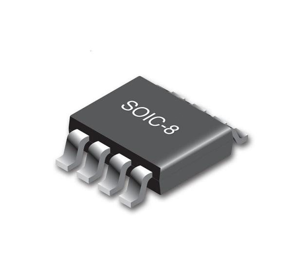
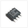
Features: • Internal DCXO for continuous glitch-free operation• Zero input-output propagation delay• Low jitter (< 35 ps RMS) outputs• Low output-output skew (< 200 ps)• 1 MHz200 MHz reference input• Supports industry standard input crystals• 200 MHz...
CY23FS08: Features: • Internal DCXO for continuous glitch-free operation• Zero input-output propagation delay• Low jitter (< 35 ps RMS) outputs• Low output-output skew (< 200 ps)...
SeekIC Buyer Protection PLUS - newly updated for 2013!
268 Transactions
All payment methods are secure and covered by SeekIC Buyer Protection PLUS.
The CY23FS08 is a FailSafe™ Zero Delay Buffer with two reference clock inputs and eight phase-aligned outputs. The device provides an optimum solution for applications where continuous operation is required in the event of a primary clock failure.
Continuous, glitch-free operation is achieved by using a DCXO, which serves as a redundant clock source in the event of a reference clock failure by maintaining the last frequency and phase information of the reference clock.
The unique feature of the CY23FS08 is that the DCXO is in fact the primary clocking source, which is synchronized (phase-aligned) to the external reference clock. When this external clock is restored, the DCXO automatically resynchronizes to the external clock.
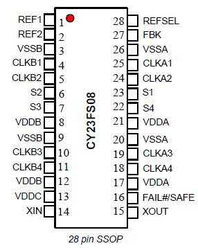
The frequency of the crystal, which will be connected to the DCXO must be chosen to be an integer factor of the frequency of the reference clock. This factor is set by four select lines: S[4:1]. please see Table 1. The CY23FS08 has three split power supplies; one for core, another for Bank A outputs and the third for Bank B outputs. Each output power supply, except VDDC can be connected to either 2.5V or 3.3V. VDDC is the power supply pin for internal circuits and must be connected to 3.3V.