Features: • Fully field-programmable
- Input and output dividers
- Inverting/noninverting outputs
- Phase-locked loop (PLL) or fanout buffer configuration
• 10-MHz to 200-MHz operating range
• Split 2.5V or 3.3V outputs
• Two LVCMOS reference inputs
• Twelve low-skew outputs
- 35ps typ. output-to-output skew (same freq)
• 110 ps typ. cycle-cycle jitter (same freq)
• Three-stateable outputs
• < 50-µA shutdown current
• Spread Aware
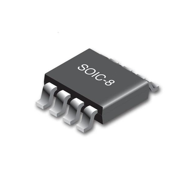
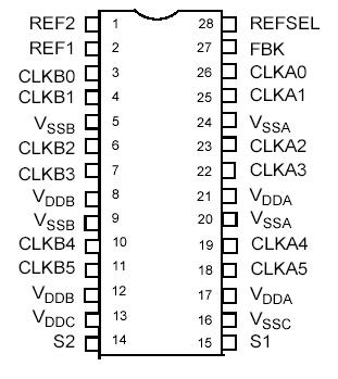
• 28-pin SSOP
• 3.3V operation
• Industrial temperature availablePinout Specifications
| Parameter |
Description |
Condition |
Min. |
Max. |
Unit |
| VDD |
Supply Voltage |
Non-functional |
0.5 |
7 |
VDC |
| VIN |
Input Voltage REF |
Relative to VCC |
0.5 |
7 |
VDC |
| VIN |
Input Voltage Except REF |
Relative to VCC |
0.5 |
VDD + 0.5 |
VDC |
| LUI |
Latch-up Immunity |
Functional |
300 |
mA |
| TS |
Temperature, Storage |
Non-functional |
65 |
+125 |
°C |
| TA |
Temperature, Operating Ambient |
Commercial Temperature |
0 |
+70 |
°C |
| TA |
Temperature, Operating Ambient |
Industrial Temperature |
40 |
+85 |
°C |
| TJ |
Junction Temperature |
Industrial Temperature |
|
125 |
°C |
| ØJc |
Dissipation, Junction to Case |
Functional |
34 |
|
°C/W |
| ØJa |
Dissipation, Junction to Ambient |
Functional |
86 |
|
°C/W |
| ESDh |
ESD Protection (Human Body Model) |
|
2000 |
V |
| MSL |
Moisture Sensitivity Level |
|
MSL 1 |
class |
| GATES |
Total Functional Gate Count |
Assembled Die |
21375 |
each |
| UL94 |
Flammability Rating |
@ 1/8 in. |
V0 |
class |
| FIT |
Failure in Time |
Manufacturing test |
10 |
ppm |
| TPU |
Power-up time for all VDDs to reach
minimum specified voltage (power
ramps must be monotonic) |
|
0.05 |
500 |
ms |
DescriptionThe CY23FP12 is a high-performance fully field-programmable 200 MHz zero delay buffer designed for high speed clock distribution. The integrated PLL is designed for low jitter and optimized for noise rejection. These parameters are critical for reference clock distribution in systems using high-performance ASICs and microprocessors.
The CY23FP12 is fully programmable via volume or prototype programmers enabling the user to define an application-specific Zero Delay Buffer with customized input and output dividers, feedback topology (internal/external), output inversions, and output drive strengths. For additional flexibility,the user can mix and match multiple functions, listed in Table 2, and assign a particular function set to any one of the four possible S1-S2 control bit combinations. This feature allows for the implementation of four distinct personalities, selectable with S1-S2 bits, on a single programmed silicon.
The CY23FP12 also features a proprietary auto-power-down circuit that shuts down the device in case of a REF failure,resulting in less than 50 µA of current draw.
The CY23FP12 provides twelve outputs grouped in two banks with separate power supply pins which can be connected independently to either a 2.5V or a 3.3V rail. Selectable reference input is a fault tolerance feature which allows for glitch-free switch over to secondary clock source when REFSEL is asserted/deasserted.

 CY23FP12 Data Sheet
